- 您現(xiàn)在的位置:買賣IC網(wǎng) > PDF目錄368024 > PIC16C717 (Microchip Technology Inc.) 8-Bit CMOS Microcontrollers(8位CMOS微控制器) PDF資料下載
參數(shù)資料
| 型號: | PIC16C717 |
| 廠商: | Microchip Technology Inc. |
| 英文描述: | 8-Bit CMOS Microcontrollers(8位CMOS微控制器) |
| 中文描述: | 8位CMOS微控制器(8位的CMOS微控制器) |
| 文件頁數(shù): | 13/220頁 |
| 文件大小: | 3585K |
| 代理商: | PIC16C717 |
第1頁第2頁第3頁第4頁第5頁第6頁第7頁第8頁第9頁第10頁第11頁第12頁當前第13頁第14頁第15頁第16頁第17頁第18頁第19頁第20頁第21頁第22頁第23頁第24頁第25頁第26頁第27頁第28頁第29頁第30頁第31頁第32頁第33頁第34頁第35頁第36頁第37頁第38頁第39頁第40頁第41頁第42頁第43頁第44頁第45頁第46頁第47頁第48頁第49頁第50頁第51頁第52頁第53頁第54頁第55頁第56頁第57頁第58頁第59頁第60頁第61頁第62頁第63頁第64頁第65頁第66頁第67頁第68頁第69頁第70頁第71頁第72頁第73頁第74頁第75頁第76頁第77頁第78頁第79頁第80頁第81頁第82頁第83頁第84頁第85頁第86頁第87頁第88頁第89頁第90頁第91頁第92頁第93頁第94頁第95頁第96頁第97頁第98頁第99頁第100頁第101頁第102頁第103頁第104頁第105頁第106頁第107頁第108頁第109頁第110頁第111頁第112頁第113頁第114頁第115頁第116頁第117頁第118頁第119頁第120頁第121頁第122頁第123頁第124頁第125頁第126頁第127頁第128頁第129頁第130頁第131頁第132頁第133頁第134頁第135頁第136頁第137頁第138頁第139頁第140頁第141頁第142頁第143頁第144頁第145頁第146頁第147頁第148頁第149頁第150頁第151頁第152頁第153頁第154頁第155頁第156頁第157頁第158頁第159頁第160頁第161頁第162頁第163頁第164頁第165頁第166頁第167頁第168頁第169頁第170頁第171頁第172頁第173頁第174頁第175頁第176頁第177頁第178頁第179頁第180頁第181頁第182頁第183頁第184頁第185頁第186頁第187頁第188頁第189頁第190頁第191頁第192頁第193頁第194頁第195頁第196頁第197頁第198頁第199頁第200頁第201頁第202頁第203頁第204頁第205頁第206頁第207頁第208頁第209頁第210頁第211頁第212頁第213頁第214頁第215頁第216頁第217頁第218頁第219頁第220頁
2002 Microchip Technology Inc.
DS41120B-page 11
PIC16C717/770/771
2.2.2
SPECIAL FUNCTION REGISTERS
The Special Function Registers are registers used by
the CPU and Peripheral Modules for controlling the
desired operation of the device. These registers are
implemented as static RAM. A list of these registers is
given in Table 2-1.
The special function registers can be classified into two
sets; core (CPU) and peripheral. Those registers asso-
ciated with the core functions are described in detail in
this section. Those related to the operation of the
peripheral features are described in detail in that
peripheral feature section.
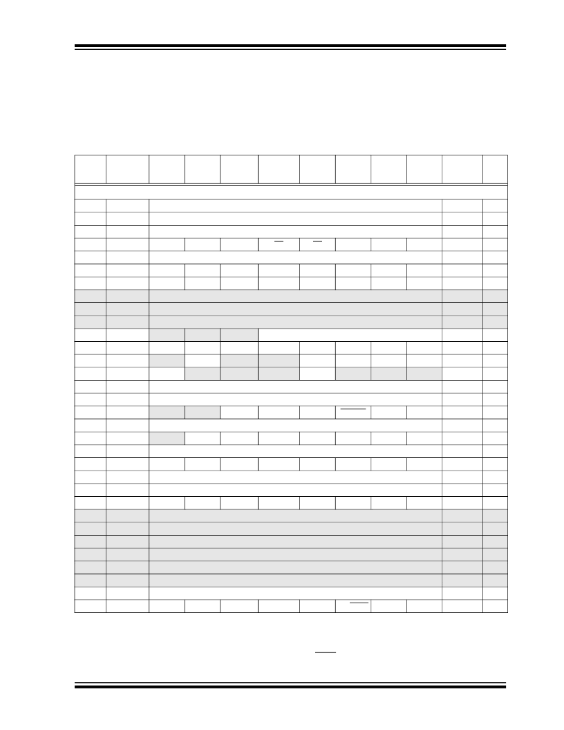
TABLE 2-1:
PIC16C717/770/771 SPECIAL FUNCTION REGISTER SUMMARY
Address Name
Bit 7
Bit 6
Bit 5
Bit 4
Bit 3
Bit 2
Bit 1
Bit 0
Value on:
POR,
BOR
Details
on
Page:
Bank 0
00h
(3)
INDF
Addressing this location uses contents of FSR to address data memory (not a physical register)
0000 0000
23
01h
TMR0
Timer0 module
’
s register
xxxx xxxx
45
02h
(3)
PCL
Program Counter's (PC) Least Significant Byte
0000 0000
22
03h
(3)
STATUS
IRP
RP1
RP0
TO
PD
Z
DC
C
0001 1xxx
14
04h
(3)
FSR
Indirect data memory address pointer
xxxx xxxx
23
05h
PORTA
RA7
RA6
RA5
RA4
RA3
RA2
RA1
RA0
xxxx 0000
25
06h
PORTB
RB7
RB6
RB5
RB4
RB3
RB2
RB1
RB0
xxxx xx11
33
07h
—
Unimplemented
—
—
08h
—
Unimplemented
—
—
09h
—
Unimplemented
—
—
0Ah
(1,3)
PCLATH
—
—
—
Write Buffer for the upper 5 bits of the Program Counter
---0 0000
22
0Bh
(3)
INTCON
GIE
PEIE
T0IE
INTE
RBIE
T0IF
INTF
RBIF
0000 000x
16
0Ch
PIR1
—
ADIF
—
—
SSPIF
CCP1IF
TMR2IF
TMR1IF
-0---0000
18
0Dh
PIR2
LVDIF
—
—
—
BCLIF
—
—
—
0--- 0---
20
0Eh
TMR1L
Holding register for the Least Significant Byte of the 16-bit TMR1 register
xxxx xxxx
47
0Fh
TMR1H
Holding register for the Most Significant Byte of the 16-bit TMR1 register
xxxx xxxx
47
10h
T1CON
—
—
T1CKPS1
T1CKPS0
T1OSCEN
T1SYNC
TMR1CS
TMR1ON
--00 0000
47
11h
TMR2
Timer2 module
’
s register
0000 0000
51
12h
T2CON
—
TOUTPS3
TOUTPS2
TOUTPS1
TOUTPS0
TMR2ON
T2CKPS1
T2CKPS0
-000 0000
51
13h
SSPBUF
Synchronous Serial Port Receive Buffer/Transmit Register
xxxx xxxx
70
14h
SSPCON
WCOL
SSPOV
SSPEN
CKP
SSPM3
SSPM2
SSPM1
SSPM0
0000 0000
67
15h
CCPR1L
Capture/Compare/PWM Register1 (LSB)
xxxx xxxx
54
16h
CCPR1H
Capture/Compare/PWM Register1 (MSB)
xxxx xxxx
54
17h
CCP1CON
PWM1M1
PWM1M0
DC1B1
DC1B0
CCP1M3
CCP1M2
CCP1M1
CCP1M0
0000 0000
53
18h
—
Unimplemented
—
—
19h
—
Unimplemented
—
—
1Ah
—
Unimplemented
—
—
1Bh
—
Unimplemented
—
—
1Ch
—
Unimplemented
—
—
1Dh
—
Unimplemented
—
—
1Eh
ADRESH
A/D High Byte Result Register
xxxx xxxx
107
1Fh
ADCON0
ADCS1
ADCS0
CHS2
CHS1
CHS0
GO/DONE
CHS3
ADON
0000 0000
107
Legend:
x
= unknown,
u
= unchanged,
q
= value depends on condition, - = unimplemented read as
’
0
’
.
Shaded locations are unimplemented, read as
‘
0
’
.
Note 1:
The upper byte of the program counter is not directly accessible. PCLATH is a holding register for the PC<12:8> whose
contents are transferred to the upper byte of the program counter.
2:
Other (non Power-up) Resets include external RESET through MCLR and Watchdog Timer Reset.
3:
These registers can be addressed from any bank.
相關PDF資料 |
PDF描述 |
|---|---|
| PIC16C770 | 8-Bit CMOS Microcontrollers(8位CMOS微控制器) |
| PIC16C771 | 8-Bit CMOS Microcontrollers(8位CMOS微控制器) |
| PIC16C73A | 8-Bit CMOS Microcontrollers with A/D Converter |
| PIC16C76 | 8-Bit CMOS Microcontrollers with A/D Converter(每個I/O口有25mA驅動/吸收電流,并行從動口,2路捕捉/比較/PWM的微控制器) |
| PIC16C77 | 8-Bit CMOS Microcontrollers with A/D Converter(每個I/O口有25mA驅動/吸收電流,并行從動口,1路捕捉/比較/PWM的微控制器) |
相關代理商/技術參數(shù) |
參數(shù)描述 |
|---|---|
| PIC16C717/JW | 功能描述:8位微控制器 -MCU 3.5KB 256 RAM 16 I/O RoHS:否 制造商:Silicon Labs 核心:8051 處理器系列:C8051F39x 數(shù)據(jù)總線寬度:8 bit 最大時鐘頻率:50 MHz 程序存儲器大小:16 KB 數(shù)據(jù) RAM 大小:1 KB 片上 ADC:Yes 工作電源電壓:1.8 V to 3.6 V 工作溫度范圍:- 40 C to + 105 C 封裝 / 箱體:QFN-20 安裝風格:SMD/SMT |
| PIC16C717/P | 功能描述:8位微控制器 -MCU 3.5KB 256 RAM 16 I/O RoHS:否 制造商:Silicon Labs 核心:8051 處理器系列:C8051F39x 數(shù)據(jù)總線寬度:8 bit 最大時鐘頻率:50 MHz 程序存儲器大小:16 KB 數(shù)據(jù) RAM 大小:1 KB 片上 ADC:Yes 工作電源電壓:1.8 V to 3.6 V 工作溫度范圍:- 40 C to + 105 C 封裝 / 箱體:QFN-20 安裝風格:SMD/SMT |
| PIC16C717/P | 制造商:Microchip Technology Inc 功能描述:IC 8BIT CMOS MCU 16C717 DIP18 |
| PIC16C717/P | 制造商:Microchip Technology Inc 功能描述:Microcontroller IC Number of I/Os:16 |
| PIC16C717/PC01 | 制造商:Microchip Technology Inc 功能描述: |
發(fā)布緊急采購,3分鐘左右您將得到回復。