- 您現(xiàn)在的位置:買賣IC網(wǎng) > PDF目錄378056 > PM7384-BI (PMC-SIERRA INC) FRAME ENGINE AND DATA LINK MANAGER 84P672 PDF資料下載
參數(shù)資料
| 型號(hào): | PM7384-BI |
| 廠商: | PMC-SIERRA INC |
| 元件分類: | 微控制器/微處理器 |
| 英文描述: | FRAME ENGINE AND DATA LINK MANAGER 84P672 |
| 中文描述: | 3 CHANNEL(S), 156M bps, SERIAL COMM CONTROLLER, PBGA352 |
| 封裝: | 35 X 35 MM, 1.51 MM HEIGHT, SBGA-352 |
| 文件頁(yè)數(shù): | 1/2頁(yè) |
| 文件大?。?/td> | 44K |
| 代理商: | PM7384-BI |
PMC-1991024 (r2)
PROPRIETARY AND CONFIDENTIAL TO PMC-SIERRA, INC., AND FOR ITS CUSTOMERS’ INTERNAL USE
2001 PMC-Sierra, Inc.
PM7384
PMC-Sierra,Inc.
Frame Engine and Data Link Manager
FREEDM-84P672
FEATURES
Single-chip multi-channel HDLC
controller with a 66 MHz, 32 bit PCI 2.1
compatible bus for configuration,
monitoring and transfer of packet data.
On-chip DMA controller with scatter/
gather capabilities.
Supports up to 672 bi-directional
HDLC channels assigned to a
maximum of 84 channelised or
unchannelised links conveyed via a
19.44 MHz Scalable Bandwidth
Interconnect (SBI) interface.
Data on the SBI interface is divided
into three Synchronous Payload
Envelopes (SPEs). Each SPE can be
configured independently to carry data
for either 28 T1/J1 links, 21 E1 links, or
one unchannelised DS-3 link.
Supports three bi-directional HDLC
channels each assigned to an
unchannelised link with arbitrary rate
link of up to 51.84 MHz when SYSCLK
is running at 45 MHz. Each link may be
configured individually to replace one
of the SPEs conveyed on the SBI
interface.
For each channel, the HDLC receiver
supports programmable flag sequence
detection, bit de-stuffing and frame
check sequence validation. The
receiver supports the validation of both
CRC-CCITT and CRC-32 frame check
sequences.
For each channel, the HDLC
transmitter supports programmable
flag sequence generation, bit stuffing
and frame check sequence generation.
The transmitter supports the
generation of both CRC-CCITT and
CRC-32 frame check sequences. The
transmitter also aborts packets under
the direction of the host or
automatically when the channel
underflows.
Provides 32 Kbytes of on-chip memory
for partial packet buffering in both the
transmit and receive directions. This
memory may be configured to support
a variety of different channel
configurations from a single channel
with 32 Kbytes of buffering to 672
channels, each with a minimum of 48
bytes of buffering.
Provides a standard five signal
P1149.1 JTAG test port for boundary
scan board test purposes.
Supports 3.3 Volt I/O on non-PCI
signals.
Supports 3.3 Volt PCI
signaling environment.
352 pin enhanced ball grid array
(SBGA) package.
APPLICATIONS
PPP interfaces for routers.
Internet/Edge Routers.
Frame Relay/Multiservice Switches.
Packet-based DSLAM equipment.
Remote Access Concentrators.
Multiservice Access Concentrators.
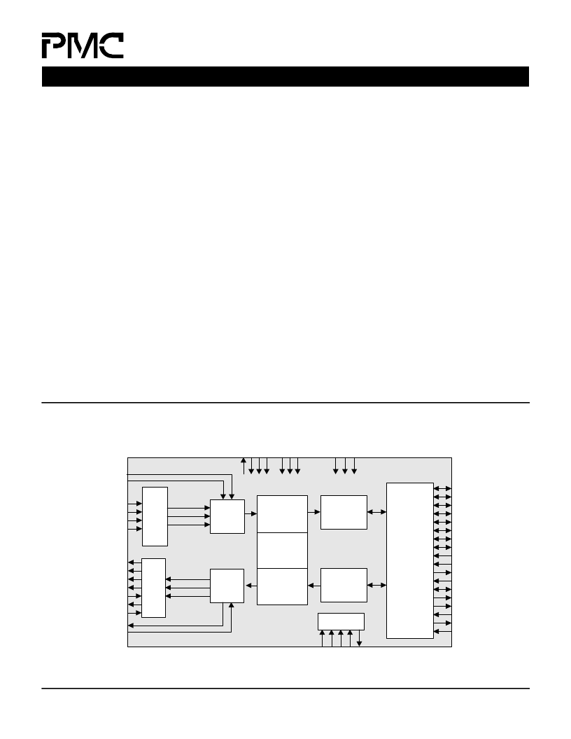
DDATA[7:0]
DPL
DV5
DDP
SBI
Extract
SBI
Insert
Transmit
HDLC Processor
(THDL672)
Performance
Monitor
(PMON)
ADATA[7:0]
APL
AV5
ADP
AJUST_REQ
AACTIVE
ADETECT[1:0]
AD[31:0]
C/BEB[3:0]
REQB
GNTB
PERRB
SERRB
PCIINTB
PCICLK
PCICLKO
M66EN
LOCKB
IDSEL
DEVSELB
STOPB
IRDYB
TRDYB
FRAMEB
PAR
R
S
P
Receive
DMA
Controller
(RMAC672)
Transmit
DMA
Controller
(TMAC672)
Receive
Channel
Assigner
(RCAS672)
Transmit
Channel
Assigner
(TCAS672)
Receive
HDLC Processor
(RHDL672)
JTAG
T
T
T
T
T
RD[2:0]
RCLK[2:0]
PCI
Controller
(GPIC672)
S
S
S
R
F
C
C
TCLK[2:0]
TD [2:0]
BLOCK DIAGRAM
相關(guān)PDF資料 |
PDF描述 |
|---|---|
| PM7385 | Frame Engine and Data Link Manager |
| PM7385-BI | 84 LINK, 672 CHANNEL FRAME ENGINE AND DATA LINK MANAGER WITH ANY-PHY PACKET INTERFACE |
| PM7388 | Frame Engine and Datalink Manager |
| PM7389 | Frame Engine and Datalink Manager |
| PM7800 | Digital Correction Signal Processor |
相關(guān)代理商/技術(shù)參數(shù) |
參數(shù)描述 |
|---|---|
| PM7385 | 制造商:PMC 制造商全稱:PMC 功能描述:Frame Engine and Data Link Manager |
| PM7385-BI | 制造商:PMC-Sierra 功能描述: |
| PM7386-BI | 制造商:Rochester Electronics LLC 功能描述: 制造商:PMC-Sierra 功能描述: |
| PM7388 | 制造商:PMC 制造商全稱:PMC 功能描述:Frame Engine and Datalink Manager |
發(fā)布緊急采購(gòu),3分鐘左右您將得到回復(fù)。