- 您現(xiàn)在的位置:買賣IC網(wǎng) > PDF目錄368082 > PN531 (NXP Semiconductors N.V.) Zener Diode; Application: General; Pd (mW): 400; Vz (V): 7.5 to 7.9; Condition Iz at Vz (mA): 5; C (pF) max: -; Condition VR at C (V):   ESD (kV) min: -; Package: MHD PDF資料下載
參數(shù)資料
| 型號: | PN531 |
| 廠商: | NXP Semiconductors N.V. |
| 英文描述: | Zener Diode; Application: General; Pd (mW): 400; Vz (V): 7.5 to 7.9; Condition Iz at Vz (mA): 5; C (pF) max: -; Condition VR at C (V):   ESD (kV) min: -; Package: MHD |
| 中文描述: | レ基于C傳輸模塊 |
| 文件頁數(shù): | 9/19頁 |
| 文件大?。?/td> | 246K |
| 代理商: | PN531 |
Philips Semiconductors Objective Short Form Specification Rev. 2.0 February 2004
PN531
μC based Transmission module
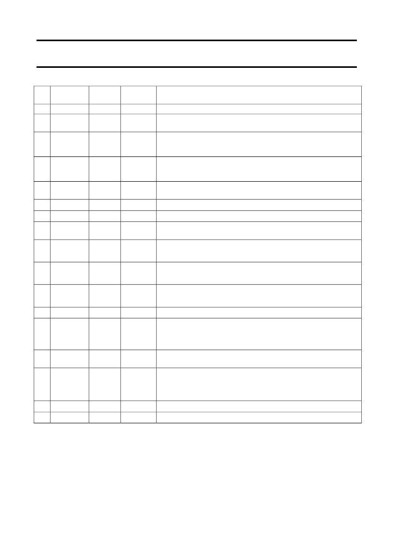
Pin
Symbol
Type
Pad Ref
Voltage
Description
this signal is used as test signal input.
25
SVDD
PWR
Connected to SAM power supply; used as a reference for communication
with the SAM.
26
P31
IO
PVDD
General purpose IO signal. Can be configured to act either as TX line of
the second serial interface or general purpose IO. In test mode this signal
is used as input and output test signal.
27
P30
IO
PVDD
General purpose IO signal. Can be configured to act either as RX line of
the second serial interface or general purpose IO. In test mode this signal
is used as input and output test signal.
28
IRQ
O
PVDD
Interrupt request: Output to signal an interrupt event to the host (Port 7 bit
0)
29
RSTOUT
IO
PVDD
Output reset signal. When Low it indicates that the circuit is in reset state.
30
DELATT
O
PVDD
Optional output for an external 1.5 KOhms resistor connection on D+.
31
NSS
IO
PVDD
Not Slave Select. In test mode this signal is used as input and output test
signal.
32
MOSI
IO
PVDD
Master Out Slave In. In test mode this signal is used as input and output
test signal
33
MISO
IO
PVDD
Master In Slave Out. In test mode this signal is used as input and output
test signal
34
SCK
IO
PVDD
Serial interface clock. In test mode this signal is used as input and output
test signal
35
PVDD
PWR
Pad power supply
In test mode this signal is used as input and output test signal.
General purpose IO signal. Can also be used as an interrupt source In test
mode this signal is used as input and output test signal.
36
P33_INT1
IO
PVDD
General purpose IO signal. Can be used to generate an HZ state on the
output of the selected interface for the Host communication and to enter
TAMA into power down mode without resetting the internal state of TAMA.
37
P32_INT0
IO
PVDD
38
RSTPD
I
PVDD
Reset and Power Down: When High, internal current sources are switched
off, the oscillator is inhibited, and the input pads are disconnected from the
outside world. With a positive edge on this pin the internal reset phase
starts.
39
DVDD
PWR
Digital Power Supply
40
VBUS
PWR
USB power supply.
9
相關(guān)PDF資料 |
PDF描述 |
|---|---|
| PN5432 | N-Channel Switch |
| PN5433 | N-Channel Switch |
| PN5434 | N-Channel Switch |
| PN6119-18R | PROGRAMMABLE UNIJUNCTION TRANSISTOR|TO-92 |
| PN6120-18R | PROGRAMMABLE UNIJUNCTION TRANSISTOR|TO-92 |
相關(guān)代理商/技術(shù)參數(shù) |
參數(shù)描述 |
|---|---|
| PN5310A3HN/C203 | 功能描述:射頻無線雜項 COMBO ANALOG/DIGI IC RoHS:否 制造商:Texas Instruments 工作頻率:112 kHz to 205 kHz 電源電壓-最大:3.6 V 電源電壓-最小:3 V 電源電流:8 mA 最大功率耗散: 工作溫度范圍:- 40 C to + 110 C 封裝 / 箱體:VQFN-48 封裝:Reel |
| PN5310A3HN/C203,51 | 功能描述:射頻無線雜項 COMBO ANALOG/DIGI IC RoHS:否 制造商:Texas Instruments 工作頻率:112 kHz to 205 kHz 電源電壓-最大:3.6 V 電源電壓-最小:3 V 電源電流:8 mA 最大功率耗散: 工作溫度范圍:- 40 C to + 110 C 封裝 / 箱體:VQFN-48 封裝:Reel |
| PN5310A3HN/C203,518 | 制造商:NXP Semiconductors 功能描述: |
| PN5310A3HN/C203,55 | 功能描述:射頻無線雜項 COMBO ANALOG/DIGI IC RoHS:否 制造商:Texas Instruments 工作頻率:112 kHz to 205 kHz 電源電壓-最大:3.6 V 電源電壓-最小:3 V 電源電流:8 mA 最大功率耗散: 工作溫度范圍:- 40 C to + 110 C 封裝 / 箱體:VQFN-48 封裝:Reel |
| PN5310A3HN/C203,551 | 制造商:NXP Semiconductors 功能描述: |
發(fā)布緊急采購,3分鐘左右您將得到回復(fù)。