- 您現(xiàn)在的位置:買賣IC網(wǎng) > PDF目錄368096 > PPC440EP (Applied Micro Circuits Corp.) Power PC 440EP Embedded Processor PDF資料下載
參數(shù)資料
| 型號: | PPC440EP |
| 廠商: | Applied Micro Circuits Corp. |
| 英文描述: | Power PC 440EP Embedded Processor |
| 中文描述: | 440EP的Power PC嵌入式處理器 |
| 文件頁數(shù): | 74/84頁 |
| 文件大?。?/td> | 541K |
| 代理商: | PPC440EP |
第1頁第2頁第3頁第4頁第5頁第6頁第7頁第8頁第9頁第10頁第11頁第12頁第13頁第14頁第15頁第16頁第17頁第18頁第19頁第20頁第21頁第22頁第23頁第24頁第25頁第26頁第27頁第28頁第29頁第30頁第31頁第32頁第33頁第34頁第35頁第36頁第37頁第38頁第39頁第40頁第41頁第42頁第43頁第44頁第45頁第46頁第47頁第48頁第49頁第50頁第51頁第52頁第53頁第54頁第55頁第56頁第57頁第58頁第59頁第60頁第61頁第62頁第63頁第64頁第65頁第66頁第67頁第68頁第69頁第70頁第71頁第72頁第73頁當(dāng)前第74頁第75頁第76頁第77頁第78頁第79頁第80頁第81頁第82頁第83頁第84頁
74
AMCC Proprietary
440EP – PPC440EP Embedded Processor
Revision 1.26 – April 25, 2007
Data Sheet
Note:
The timing data in the following tables is based on simulation runs using Einstimer.
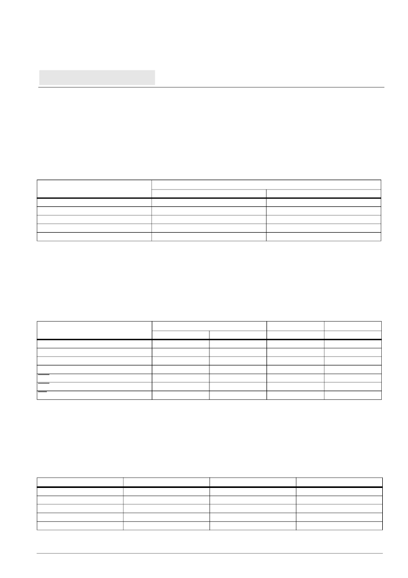
Table 19. I/O Timing—DDR SDRAM T
DS
Notes:
1. All of the DQS signals are referenced to MemClkOut0(0).
2. Clock speed is 133MHz.
3. The T
DS
values in the table include 3/4 of a cycle at 133MHz (7.5ns x 0.75 = 5.625 ns).
4. To obtain adjusted values for lower clock frequencies, subtract 5.625 ns from the values in the table and add 3/4 of the cycle
time for the lower clock frequency (T
DS
- 5.625 + 0.75T
CYC
).
Table 20. I/O Timing—DDR SDRAM T
SK
, T
SA
, and T
HA
Notes:
1. Clock speed is 133MHz. T
SK
is referenced to MemClkOut0(0). T
SA
and T
HA
are referenced to MemClkOut0(90).
2. To obtain adjusted T
SA
values for lower clock frequencies, use 3/4 of the cycle time for the lower clock frequency and subtract
T
SK
maximum (0.75T
CYC
- T
SK
max).
3. To obtain adjusted T
HA
values for lower clock frequencies, use 1/4 of the cycle time for the lower clock frequency and add
T
SK
minimum (0.25T
CYC
+ T
SK
min).
Table 21. I/O Timing—DDR SDRAM T
SD
and T
HD
Notes:
1. T
SD
and T
HD
are measured under worst case conditions.
2. Clock speed for the values in the table is 133MHz.
3. The time values in the table include 1/4 of a cycle at 133MHz (7.5ns x 0.25 = 1.875 ns).
4. To obtain adjusted T
SD
and T
HD
values for lower clock frequencies, subtract 1.875 ns from the values in the table and add
1/4 of the cycle time for the lower clock frequency (e.g., T
SD
- 1.875 + 0.25T
CYC
).
Signal Name
T
DS
(ns)
Minimum
5.76
5.78
5.82
5.79
5.75
Maximum
5.86
5.91
5.90
5.89
5.88
DQS0
DQS1
DQS2
DQS3
DQS8
Signal Name
T
SK
(ns)
T
SA
(ns)
Minimum
5.31
5.32
5.38
5.35
5.32
5.35
5.41
T
HA
(ns)
Minimum
1.99
1.95
1.93
1.95
1.93
1.93
1.96
Minimum
0.11
0.07
0.05
0.07
0.05
0.05
0.08
Maximum
0.32
0.31
0.25
0.28
0.31
0.28
0.22
MemAddr00:12
BA0:1
BankSel0:3
ClkEn0:3
CAS
RAS
WE
Signal Names
Reference Signal
DQS0
DQS1
DQS2
DQS3
DQS8
T
SD
(ns)
1.795
1.775
1.745
1.765
1.685
T
HD
(ns)
1.866
1.865
1.862
1.864
1.857
MemData00:07, DM0
MemData08:15, DM1
MemData16:23, DM2
MemData24:31, DM3
ECC0:7, DM8
相關(guān)PDF資料 |
PDF描述 |
|---|---|
| PPC440EP-3pbfffCx | Power PC 440EP Embedded Processor |
| PPC440GP-3CC333C | Power PC 440GP Embedded Processor |
| PPC440GP-3CC400C | Power PC 440GP Embedded Processor |
| PPC440GP-3CC400CZ | Power PC 440GP Embedded Processor |
| PPC440GP-3CC400E | Power PC 440GP Embedded Processor |
相關(guān)代理商/技術(shù)參數(shù) |
參數(shù)描述 |
|---|---|
| PPC440EP-3BB533C | 制造商:AppliedMicro 功能描述: |
| PPC440EP-3BC400C | 制造商:AMCC 功能描述:MPU 440EP RISC 16BIT 0.13UM 400MHZ 3.3V 456PIN EBGA - Trays 制造商:AMCC 功能描述:AMCPPC440EP-3BC400C APD BIAS CTRL/MONITR |
| PPC440EP-3BC533C | 制造商:AppliedMicro 功能描述:MPU 440EP RISC 16-Bit 0.13um 533MHz 3.3V 456-Pin EBGA Tray |
| PPC440EP-3JA333CZ | 制造商:AppliedMicro 功能描述: |
| PPC440EP-3JA400C | 制造商:AppliedMicro 功能描述: |
發(fā)布緊急采購,3分鐘左右您將得到回復(fù)。