- 您現(xiàn)在的位置:買(mǎi)賣IC網(wǎng) > PDF目錄372668 > XC6111A341 (TOREX SEMICONDUCTOR LTD.) CMOS Voltage Detector PDF資料下載
參數(shù)資料
| 型號(hào): | XC6111A341 |
| 廠商: | TOREX SEMICONDUCTOR LTD. |
| 英文描述: | CMOS Voltage Detector |
| 中文描述: | CMOS電壓檢測(cè)器 |
| 文件頁(yè)數(shù): | 10/26頁(yè) |
| 文件大小: | 535K |
| 代理商: | XC6111A341 |
第1頁(yè)第2頁(yè)第3頁(yè)第4頁(yè)第5頁(yè)第6頁(yè)第7頁(yè)第8頁(yè)第9頁(yè)當(dāng)前第10頁(yè)第11頁(yè)第12頁(yè)第13頁(yè)第14頁(yè)第15頁(yè)第16頁(yè)第17頁(yè)第18頁(yè)第19頁(yè)第20頁(yè)第21頁(yè)第22頁(yè)第23頁(yè)第24頁(yè)第25頁(yè)第26頁(yè)
XC6101~XC6107, XC6111~XC6117 Series
10/26
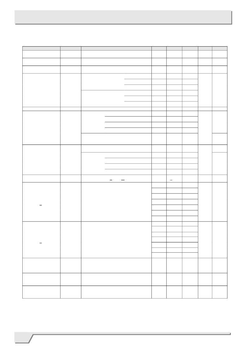
NOTE:
*1: XC6101~XC6107 (with hysteresis)
*2: XC6111~XC6117 (without hysteresis)
*3: ‘X’ represents both ‘0’ and ‘1’. (ex. XC61X1
XC6101 and XC6111)
*4: V
DF(T)
: Setting detect voltage
*5: If only “V
DF
” is indicated, it represents both V
DFL
(low when detected) and V
DFH
(high when detected).
PARAMETER
Detect Voltage
Hysteresis Range
XC6101~XC6107 (*1)
Hysteresis Range
XC6111~XC6117 (*2)
SYMBOL
V
DFL
V
DFH
V
HYS
CONDITIONS
MIN.
V
DF(T)
× 0.98
V
DF
× 0.02
0
TYP.
V
DF(T)
V
DF
× 0.05
V
DF
× 0.001
5
10
12
4
8
10
-
0.5
2.5
3.5
4.0
MAX.
V
DF(T)
× 1.02
V
DF
× 0.08
V
DF
x 0.01
11
16
18
10
14
16
6.0
-
-
-
-
UNITS
CIRCUIT
V
1
V
1
V
HYS
V
1
V
IN
=V
DF(T)
×0.9V
-
-
-
-
-
-
V
IN
=V
DF(T)
×1.1V
V
IN
=6.0V
XC61X1/XC61X2/XC61X3
XC61X4/XC61X5 (*3)
(The MRB & the WD Pin:
No connection)
V
IN
=V
DF(T)
×0.9V
V
IN
=V
DF(T)
×1.1V
V
IN
=6.0V
Supply Current
I
SS
XC61X6/XC61X7 (*3)
(The MRB Pin:
No connection)
μ
A
2
Operating Voltage
V
IN
1.0
0.15
2.0
3.0
3.5
V
1
VIN=1.0V
V
IN
=2.0V (V
DFL(T)
> 2.0V)
V
IN
=3.0V (V
DFL(T)
>3.0V)
V
IN
=4.0V (V
DFL(T)
>4.0V)
N-ch.
V
DS
= 0.5V
3
V
DFL
Output Current
(RESETB)
I
RBOUT
CMOS,
P-ch
V
DS
= 0.5V
N-ch
V
DS
= 0.5V
V
IN
=6.0V
-
- 1.1
-0.8
mA
4
V
IN
=6.0V
4.4
4.9
-
3
V
IN
=1.0V
-
-
-
-
- 0.08
- 0.50
- 0.75
- 0.95
- 0.02
- 0.30
- 0.55
- 0.75
V
IN
=2.0V (V
DFH(T)
> 2.0V)
V
IN
=3.0V (V
DFH(T)
>3.0V)
V
IN
=4.0V (V
DFH(T)
>4.0V)
-40
O
C < Topr < 85
O
C
V
DFH
Output Current
(RESET)
I
ROUT
P-ch.
V
DS
= 0.5V
mA
4
Temperature
Characteristics
△
V
DF
/
△
Topr
V
DF
-
+100
-
ppm
/
O
C
1
2
13
25
60
120
240
960
2
13
25
60
120
240
960
3.13
25
50
100
200
400
1600
3.13
25
50
100
200
400
1600
5
38
75
140
280
560
2240
5
38
75
140
280
560
2240
Release Delay Time
(V
DF
<1.8V)
T
DR
Time until V
IN
is increased from
1.0V to 2.0V
and attains to the release
time level,
and the Reset output pin inverts.
ms
5
Release Delay Time
(V
DF
>1.9V)
T
DR
Time until V
IN
is increased from
1.0V to (V
DF
x1.1V)
and attains to the release
time level,
and the Reset output pin inverts.
ms
5
Detect Delay Time
T
DF
Time until V
IN
is decreased from 6.0V to
1.0V and attains to the detect voltage
level, and the Reset output pin detects
while the WD pin left opened.
-
3
30
μ
s
5
V
DFL
/V
DFH
CMOS Output
Leak Current
V
DFL
N-ch Open Drain
Output
Leak Current
I
LEAK
V
IN
=6.0V, RESETB=6.0V (V
DFL
)
V
IN
=6.0V, RESET=0V (V
DFH
)
-
0.01
-
μ
A
3
I
LEAK
V
IN
=6.0V, RESETB=6.0V
-
0.01
0.10
μ
A
3
■
ELECTRICAL CHARACTERISTICS
●
XC6101~XC6107, XC6111~XC6117 Series
Ta = 25
O
C
相關(guān)PDF資料 |
PDF描述 |
|---|---|
| XC6111A342 | CMOS Voltage Detector |
| XC6111A343 | CMOS Voltage Detector |
| XC6111A344 | CMOS Voltage Detector |
| XC6111A345 | CMOS Voltage Detector |
| XC6111A346 | CMOS Voltage Detector |
相關(guān)代理商/技術(shù)參數(shù) |
參數(shù)描述 |
|---|---|
| XC6115B230MR-G | 制造商:Torex Semiconductor LTD 功能描述: |
| XC6115B330MRN | 制造商:Torex Semiconductor LTD 功能描述: |
| XC6118N09AMR-G | 制造商:Torex Semiconductor LTD 功能描述: |
| XC6118N10AMR-G | 制造商:Torex Semiconductor LTD 功能描述: |
| XC6118N13AMR-G | 制造商:Torex Semiconductor LTD 功能描述: |
發(fā)布緊急采購(gòu),3分鐘左右您將得到回復(fù)。