- 您現(xiàn)在的位置:買賣IC網(wǎng) > PDF目錄98066 > PTV03020WAH (TEXAS INSTRUMENTS INC) 1-OUTPUT DC-DC REG PWR SUPPLY MODULE PDF資料下載
參數(shù)資料
| 型號: | PTV03020WAH |
| 廠商: | TEXAS INSTRUMENTS INC |
| 元件分類: | 電源模塊 |
| 英文描述: | 1-OUTPUT DC-DC REG PWR SUPPLY MODULE |
| 封裝: | SIP-12 |
| 文件頁數(shù): | 18/19頁 |
| 文件大?。?/td> | 434K |
| 代理商: | PTV03020WAH |
www.ti.com
Designing for Fast Load Transients
Adjusting the Output Voltage
R
SET + 10 kW
0.8 V
V
O * 0.8 V
* 2.49 kW
(1)
SLTS243A – FEBRUARY 2005 – REVISED OCTOBER 2007
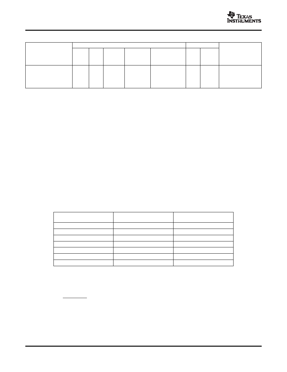
Table 1. Input/Output Capacitors (continued)
Capacitor Characteristics
Quantity
Max Ripple
Capacitor Vendor,
Vendor
Working
Max ESR
Optional
Value
Current at
Physical Size
Input
Type/Series (Style)
Part Number
Voltage
at 100 kHz
Output
(F)
85
°C (Irms)
(mm)
Bus
(V)
(
)
Bus
(mA)
TDK, Ceramic X5R (SMD)
6.3
100
0.002
—
3225
≥1(3)
≤ 3
C3225X5R0J107MT
6.3
47
≥1 (3)
≤ 5
C3225X5R0J476MT
16
22
≥1 (3)
≤ 5
C3225X5R1C226MT
16
10
≥2 (3)
≤ 5
C3225X5R1C106MT
The transient response of the dc/dc converter has been characterized using a load transient with a di/dt of
1 A/s. The typical voltage deviation for this load transient is given in the data sheet specification table using the
optional value of output capacitance. As the di/dt of a transient is increased, the response of a converter
regulation circuit ultimately depends on its output capacitor decoupling network. This is an inherent limitation with
any dc/dc converter once the speed of the transient exceeds its bandwidth capability. If the target application
specifies a higher di/dt or lower voltage deviation, the requirement can only be met with additional output
capacitor decoupling. In these cases special attention must be paid to the type, value, and ESR of the capacitors
selected.
If the transient performance requirements exceed that specified in the data sheet, or the total amount of load
capacitance is above 3000 F, the selection of output capacitors becomes more important.
The VO Adjust control (pin 8) sets the output voltage of the PTV03020W product to a value over the range, 0.8 V
to 2.5 V. The adjustment method requires the addition of a single external resistor, RSET, that must be connected
directly between the VO Adjust and the regulator's output GND (pin 1 or 2). Without an adjust resistor, the output
voltage is set to its lowest value. Table 2 gives the preferred value of the external resistor for a number of
standard voltages, along with the actual output voltage that this resistance value provides. Figure 6 shows the
placement of the required resistor.
Table 2. Nearest Standard Values of RSET for Common Output Voltages
VO
RSET
VO
(Required)
(Standard Value)
(Actual)
2.5 V (1)
2.21 k
2.502 V
2 V
4.12 k
2.010 V
1.8 V
5.49 k
1.803 V
1.5 V
8.87 k
1.504 V
1.2 V
17.4 k
1.202 V
1 V
36.5 k
1.005 V
0.8 V
Open
0.800 V
(1)
For VO =2.5 V, the minimum input voltage is 3.15 V. See Electrical Characteristics for additional
information.
For other output voltages, the value of the required resistor can either be calculated or simply selected from the
range of values given in Table 3. Equation 1 may be used for calculating the adjust resistor value.
8
Copyright 2005–2007, Texas Instruments Incorporated
Product Folder Link(s) :PTV03020W
相關(guān)PDF資料 |
PDF描述 |
|---|---|
| PTV05010WAH | 1-OUTPUT DC-DC REG PWR SUPPLY MODULE |
| PTV08T250WAH | 1-OUTPUT DC-DC REG PWR SUPPLY MODULE |
| PTV08T250WAD | 1-OUTPUT DC-DC REG PWR SUPPLY MODULE |
| PTV12010WAD | 1-OUTPUT DC-DC REG PWR SUPPLY MODULE |
| PTV12010WAH | 1-OUTPUT DC-DC REG PWR SUPPLY MODULE |
相關(guān)代理商/技術(shù)參數(shù) |
參數(shù)描述 |
|---|---|
| PTV05010 | 制造商:ARTESYN 制造商全稱:Artesyn Technologies 功能描述:DC-DC CONVERTERS POLA Non-isolated |
| PTV05010W | 制造商:TI 制造商全稱:Texas Instruments 功能描述:8-A, 5-V INPUT NONISOLATED WIDE-OUTPUT ADJUST SIP MODULE |
| PTV05010WAD | 功能描述:DC/DC轉(zhuǎn)換器 28.8W 0.8-3.6V 8A RoHS:否 制造商:Murata 產(chǎn)品: 輸出功率: 輸入電壓范圍:3.6 V to 5.5 V 輸入電壓(標(biāo)稱): 輸出端數(shù)量:1 輸出電壓(通道 1):3.3 V 輸出電流(通道 1):600 mA 輸出電壓(通道 2): 輸出電流(通道 2): 安裝風(fēng)格:SMD/SMT 封裝 / 箱體尺寸: |
| PTV05010WAH | 功能描述:DC/DC轉(zhuǎn)換器 8A 5V-In Wide-Out Adj SIP Module RoHS:否 制造商:Murata 產(chǎn)品: 輸出功率: 輸入電壓范圍:3.6 V to 5.5 V 輸入電壓(標(biāo)稱): 輸出端數(shù)量:1 輸出電壓(通道 1):3.3 V 輸出電流(通道 1):600 mA 輸出電壓(通道 2): 輸出電流(通道 2): 安裝風(fēng)格:SMD/SMT 封裝 / 箱體尺寸: |
| PTV05020 | 制造商:EMERSON-NETWORKPOWER 制造商全稱:Emerson Network Power 功能描述:DC-DC CONVERTERS |
發(fā)布緊急采購,3分鐘左右您將得到回復(fù)。