- 您現(xiàn)在的位置:買賣IC網(wǎng) > PDF目錄361317 > QS5LV91970Q (INTEGRATED DEVICE TECHNOLOGY INC) 3.3V LOW SKEW CMOS PLL CLOCK DRIVER WITH INTEGRATED LOOP FILTER PDF資料下載
參數(shù)資料
| 型號: | QS5LV91970Q |
| 廠商: | INTEGRATED DEVICE TECHNOLOGY INC |
| 元件分類: | 時鐘及定時 |
| 英文描述: | 3.3V LOW SKEW CMOS PLL CLOCK DRIVER WITH INTEGRATED LOOP FILTER |
| 中文描述: | 5LV SERIES, PLL BASED CLOCK DRIVER, 7 TRUE OUTPUT(S), 1 INVERTED OUTPUT(S), PDSO28 |
| 封裝: | QSOP-28 |
| 文件頁數(shù): | 8/12頁 |
| 文件大小: | 98K |
| 代理商: | QS5LV91970Q |

8
INDUSTRIAL TEMPERATURE RANGE
QS5LV919
3.3V LOW SKEW CMOS PLL CLOCK DRIVER WITH INTEGRATED LOOP FILTER
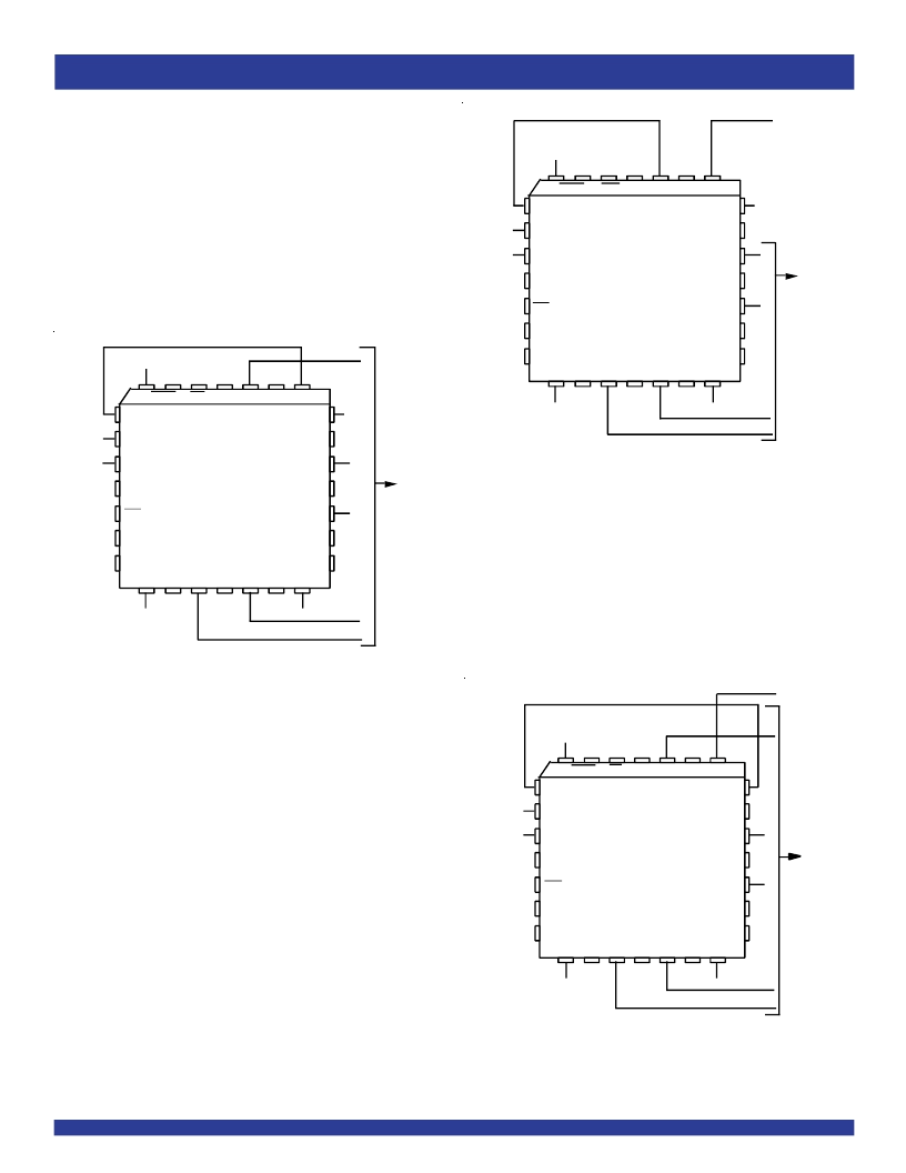
The frequency relationship shown here is applicable to all Q outputs (Q0, Q1,
Q2, Q3 and Q4).
1:2 INPUT TO "Q" OUTPUT FREQUENCY RELATIONSHIP
In this application, the Q/2 output is connected to the FEEDBACK input. The
internal PLL will line up the positive edges of Q/2 and SYNC, thus the Q/2
frequency will equal the SYNC frequency. The Q outputs (Q0-Q4,
Q5
) will
always run at 2X the Q/2 frequency, and the 2Q output will run at 4X the Q/2
frequency.
Allowable Input Frequency Range:
20MHz to (f2Q MAX Spec)/2 (for FREQ_SEL HIGH)
10MHz to (f2Q MAX Spec)/4 (for FREQ_SEL LOW)
Figure 2c. Wiring Diagram and Frequency Relationships with
Q2 Output Feedback
Figure 2b. Wiring Diagram and Frequency Relationships with
Q4 Output Feedback
Allowable Input Frequency Range:
10MHz to ( f2Q MAX Spec)/4 (for FREQ_SEL HIGH)
5MHz to (f2Q MAX Spec)/8 (for FREQ_SEL LOW)
Q/2
Q3
Q2
PLL_EN
Q1
Q0
FQ_SEL
FEEDBACK
REF_SEL
SYNC(0)
V
CC
(AN)
GND(AN)
Q4
Q5
2Q
LOW
50 MHz signal
12.5 MHz feedback signal
HIGH
HIGH
HIGH
25 MHz
"Q"
Clock
Outputs
12.5 MHz
input
PE
QS5LV919
RST
OE/
Q/2
Q3
Q2
PLL_EN
Q1
Q0
FQ_SEL
FEEDBACK
REF_SEL
SYNC(0)
V
CC
(AN)
GND(AN)
Q4
Q5
2Q
LOW
50 MHz signal
25 MHz feedback signal
HIGH
HIGH
HIGH
25 MHz
"Q"
Clock
Outputs
25 MHz
input
12.5 MHz
signal
PE
QS5LV919
RST
OE/
Allowable Input Frequency Range:
40MHz to (f2Q MAX Spec) (for FREQ_SEL HIGH)
20MHz to (f2Q MAX Spec)/2 (for FREQ_SEL LOW)
2:1 INPUT TO "Q" OUTPUT FREQUENCY RELATIONSHIP
In this application, the 2Q output is connected to the FEEDBACK input. The
internal PLL will line up the positive edges of 2Q and SYNC, thus the 2Q
frequency will equal the SYNC frequency. The Q/2 output will always run at
1/4 the 2Q frequency, and the Q output will run at 1/2 the 2Q frequency.
Note that with 2Q as feedback, the maximuminput frequency is 100MHz for FS
= HIGH
Figure 2a. Wiring Diagram and Frequency Relationships with 2Q
Output Feedback
Q/2
Q3
Q2
PLL_EN
Q1
Q0
FQ_SEL
FEEDBACK
REF_SEL
SYNC(0)
V
CC
(AN)
GND(AN)
Q4
Q5
2Q
LOW
50 MHz feedback signal
HIGH
HIGH
HIGH
25 MHz
"Q"
Clock
Outputs
50 MHz
input
12.5 MHz
input
PE
QS5LV919
RST
OE/
1:1 INPUT TO "Q" OUTPUT FREQUENCY RELATIONSHIP
In this application, the Q4 output is connected to the FEEDBACK input. The
internal PLL will line up the positive edges of Q4 and SYNC, thus the Q4
frequency (and the rest of the "Q" outputs) will equal the SYNC frequency. The
Q/2 output will always run at 1/2 the Q frequency, and the 2Q output will run
at 2X the Q frequency.
相關(guān)PDF資料 |
PDF描述 |
|---|---|
| QS5LV919 | 3.3V LOW SKEW CMOS PLL CLOCK DRIVER WITH INTEGRATED LOOP FILTER |
| QS5LV919100J | 3.3V LOW SKEW CMOS PLL CLOCK DRIVER WITH INTEGRATED LOOP FILTER |
| QS5LV919100Q | 3.3V LOW SKEW CMOS PLL CLOCK DRIVER WITH INTEGRATED LOOP FILTER |
| QS5LV919133J | 3.3V LOW SKEW CMOS PLL CLOCK DRIVER WITH INTEGRATED LOOP FILTER |
| QS5LV931-50Q | 3.3V LOW SKEW CMOS PLL CLOCK DRIVER WITH INTEGRATED LOOP FILTER |
相關(guān)代理商/技術(shù)參數(shù) |
參數(shù)描述 |
|---|---|
| QS5LV931 | 制造商:IDT 制造商全稱:Integrated Device Technology 功能描述:3.3V LOW SKEW CMOS PLL CLOCK DRIVER WITH INTEGRATED LOOP FILTER |
| QS5LV93150Q | 制造商:IDT 制造商全稱:Integrated Device Technology 功能描述:3.3V LOW SKEW CMOS PLL CLOCK DRIVER WITH INTEGRATED LOOP FILTER |
| QS5LV931-50Q | 制造商:IDT 制造商全稱:Integrated Device Technology 功能描述:3.3V LOW SKEW CMOS PLL CLOCK DRIVER WITH INTEGRATED LOOP FILTER |
| QS5LV93166Q | 制造商:IDT 制造商全稱:Integrated Device Technology 功能描述:3.3V LOW SKEW CMOS PLL CLOCK DRIVER WITH INTEGRATED LOOP FILTER |
| QS5LV931-66Q | 制造商:IDT 制造商全稱:Integrated Device Technology 功能描述:3.3V LOW SKEW CMOS PLL CLOCK DRIVER WITH INTEGRATED LOOP FILTER |
發(fā)布緊急采購,3分鐘左右您將得到回復。