- 您現(xiàn)在的位置:買賣IC網(wǎng) > PDF目錄230913 > RDC-19220-102 (DATA DEVICE CORP) SYNCHRO OR RESOLVER TO DIGITAL CONVERTER, CDIP40 PDF資料下載
參數(shù)資料
| 型號: | RDC-19220-102 |
| 廠商: | DATA DEVICE CORP |
| 元件分類: | 位置變換器 |
| 英文描述: | SYNCHRO OR RESOLVER TO DIGITAL CONVERTER, CDIP40 |
| 封裝: | 2 X 0.600 INCH, 0.200 INCH HEIGHT, CERAMIC, DDIP-40 |
| 文件頁數(shù): | 6/24頁 |
| 文件大小: | 1233K |
| 代理商: | RDC-19220-102 |
14
Data Device Corporation
www.ddc-web.com
RDC-19220 SERIES
V-12/08-0
+S
-S
SIN
aR
R
+C
-C
COS
R
-
+
-
+
R
aR
C1
bR
2R
R
bR
+REF
-REF
R
C2
2 WIRE LVDT
REF IN
R
2 V
FS = 2 V
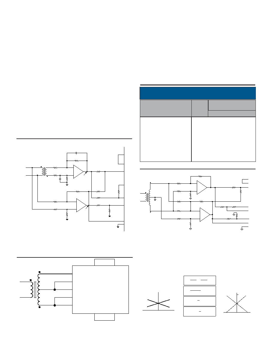
FIGURE 12A. 2-WIRE LVdT dIREcT INPUT
TABLE 7. LVdT OUTPUT cOdE (14-BIT R/d OR
12-BIT LVdT)
dATA
+ over full travel
+ full travel -1 LSB
+0.5 travel
+1 LSB
null
- 1 LSB
-0.5 travel
- full travel
- over full travel
01
xxxx
00
1111
00
1100
0000
00
1000
0000
0001
00
1000
0000
00
0111
1111
00
0100
0000
00
0000
11
xxxx
C1 = C2, set for phase lag = phase lead through the LVDT.
Note: TABLE 7 refers to FIguRE 12C.
LVDT MODE
As shown in TABLE 1 the RDC-19220 Series units can be made
to operate as LVDT-to-digital converters by connecting Resolution
Control inputs A and B to “0,” “1,” or the -5 volt supply. In this
mode the RDC-19220 Series functions as a ratiometric tracking
linear converter. When linear ac inputs are applied from a LVDT
the converter operates over one quarter of its range. This results
in two less bits of resolution for LVDT mode than are provided in
resolver mode.
FIguRE 12B shows a direct LVDT 2 Vrms full scale input. Some
LDVT output signals will need to be scaled to be compatible with
the converter input. FIguRE 12C is a schematic of an input scal-
ing circuit applicable to 3-wire LVDTs. The value of the scaling
constant “a” is selected to provide an input of 2 Vrms at full stroke
of the LVDT. The value of scaling constant “b” is selected to pro-
vide an input of 1 Vrms at null of the LVDT. Suggested compo-
nents for implementing the input scaling circuit are a quad op-
amp, such as a 4741 type, and precision film resistors of 0.1%
tolerance. FIguRE 12A illustrates a 2-wire LVDT configuration.
Data output of the RDC-19220 Series is Binary Coded in LVDT
mode. The most negative stroke of the LVDT is represented by
all zeros and the most positive stroke of the LVDT is represented
by
all ones. The most significant 2 bits (2 MSBs) may be used
as overrange indicators. Positive overrange is indicated by code
“01” and negative overrange is indicated by code “11” (see
TABLE 7).
INHIBIT, ENABLE, AND CB TIMINg
LVdT OUTPUT
MsB
LsB
OVER
RANGE
FIGURE 12B. 3-WIRE LVdT dIREcT INPUT
+S
-S
SIN
-C
COS
-REF
+REF
A GND
+C
RDC-19220
+S
-S
SIN
aR
R
+C
-C
COS
R'
-
+
-
+
R/2
R
aR
bR
2R'
R'
bR
+REF
-REF
R'
R
VB
VA
REF
-2V
FS=2V
Notes;
1. R 10k
2. Consideration for the value of R is LVDT loading.
3. RMS values given.
4. Use the absolute values of Va and Vb when subtracting per the formula for calculating
resistance values, and then use the calculated sign of "Va and Vb" for calculating SIN
and COS. The calculations shown are based upon full scale travel being to the Va side
of the LVDT.
5. See the RDC application manual for calculation examples.
6. Negative voltages are 180 phase for the reference.
FIGURE 12c. 3-WIRE LVdT scALING cIRcUIT
VB
VA
LVDT
OUTPUT
+FS
-FS
NULL
COS
SIN
RDC-19220
INPUT
-FS
+FS
NULL
1V
2V
1
V
b =
=
Anull
1
VBnull
2
(V - V )
a =
A
B
SIN=-1V+ (V - V )
A
B
a
2
COS=-1V -
(V - V )
A
B
a
2
max.
相關(guān)PDF資料 |
PDF描述 |
|---|---|
| RD-14592D1-234S | SYNCHRO OR RESOLVER TO DIGITAL CONVERTER, MDMA36 |
| RD-14592D1-242Q | SYNCHRO OR RESOLVER TO DIGITAL CONVERTER, MDMA36 |
| RD-14592D1-255 | SYNCHRO OR RESOLVER TO DIGITAL CONVERTER, MDMA36 |
| RD-14592D1-264L | SYNCHRO OR RESOLVER TO DIGITAL CONVERTER, MDMA36 |
| RD-14597F1-175L | SYNCHRO OR RESOLVER TO DIGITAL CONVERTER, CDFP36 |
相關(guān)代理商/技術(shù)參數(shù) |
參數(shù)描述 |
|---|---|
| RDC-19220-103 | 制造商:未知廠家 制造商全稱:未知廠家 功能描述:LVDT/Resolver-to-Digital Converter |
| RDC19220-111 | 制造商:未知廠家 制造商全稱:未知廠家 功能描述:Converter IC |
| RDC-19220-112 | 制造商:未知廠家 制造商全稱:未知廠家 功能描述:LVDT/Resolver-to-Digital Converter |
| RDC-19220-113 | 制造商:未知廠家 制造商全稱:未知廠家 功能描述:LVDT/Resolver-to-Digital Converter |
| RDC19220-121 | 制造商:未知廠家 制造商全稱:未知廠家 功能描述:Converter IC |
發(fā)布緊急采購,3分鐘左右您將得到回復(fù)。