- 您現(xiàn)在的位置:買(mǎi)賣(mài)IC網(wǎng) > PDF目錄385769 > RF2483 (RF MICRO DEVICES INC) LOW NOISE DUAL-BAND QUADRATURE MODULATOR WITH AGC PDF資料下載
參數(shù)資料
| 型號(hào): | RF2483 |
| 廠商: | RF MICRO DEVICES INC |
| 元件分類(lèi): | 無(wú)繩電話/電話 |
| 英文描述: | LOW NOISE DUAL-BAND QUADRATURE MODULATOR WITH AGC |
| 中文描述: | TELECOM, CELLULAR, RF AND BASEBAND CIRCUIT, QCC20 |
| 封裝: | 4 X 4 MM, ROHS COMPLIANT, QFN-20 |
| 文件頁(yè)數(shù): | 6/20頁(yè) |
| 文件大小: | 423K |
| 代理商: | RF2483 |
第1頁(yè)第2頁(yè)第3頁(yè)第4頁(yè)第5頁(yè)當(dāng)前第6頁(yè)第7頁(yè)第8頁(yè)第9頁(yè)第10頁(yè)第11頁(yè)第12頁(yè)第13頁(yè)第14頁(yè)第15頁(yè)第16頁(yè)第17頁(yè)第18頁(yè)第19頁(yè)第20頁(yè)
Preliminary
5-34
RF2483
Rev A2 010904
5
M
U
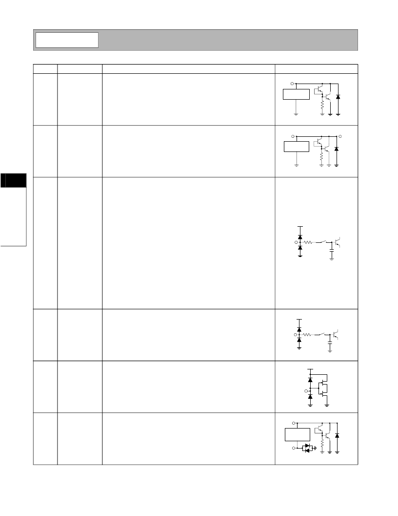
Pin
1
Function
VCC3
Description
Supply for RF output circuits.
Interface Schematic
2
VCC2
Supply for modulator and biasing circuits.
3
ISIG P
In phase I channel positive baseband input port. Best performance is
achieved when the ISIGP and ISIGN are driven differentially. The rec-
ommended CW differential drive level (V
ISIGP
-V
ISIGN
) is 800mV
P-P
.
This input should be DC-biased at 1.2V±0.05V. The common-mode
DC coltage on the ISIGP and ISIGN input signals is used to bias the
modulator. In sleep mode an internal FET switch is opened, the input
goes high impedance and the modulator is de-biased. The input imped-
ance is typically 5.5k
at low frequencies and at higher frequencies
can be modeled as 50
in series with 12pF to ground.
Phase or amplitude errors between the ISIGP and ISIGN signals may
result in the even order distortion of the modulation in the output spec-
trum.
DC offsets between the ISIGP and ISIGN signals will result in
increased carrier leakage. Small DC offsets may be deliberately
applied between the ISIGP/ISIGN and QSIGP/QSIGN inputs to cancel
out LO leakage. The optimum corrective DC offsets will change with
mode, frequency and gain control.
Common-mode noise on the ISIGP and ISGN should be kept low as it
may degrade the noise performance of the modulator.
Phase offsets may be applied between the I and Q channels to improve
the sideband suppression performance.
In phase I channel negative baseband input port. See ISIGP.
4
ISIG N
5
ENABLE
Enables power to the device.
CMOS input.
Logic 1 (1.4V to VCC)=Enabled.
Logic 0 (0V to 0.5V)=Powered Down.
6
VCC1
Supply for the LO buffers and quadrature network.
The sideband suppression is a function of the VCC1 voltage. The inclu-
sion of R3 (39
) lowers the voltage on VCC1 by around 400mV and
results an improvement in sideband suppression but around a 0.2dB
increase in noise at 20MHz offset.
VCC3
RF Output
Amplifier
VCC2
Modulator and
VGA
VCC2
V
CC2
12 pF
50
V
CC2
12 pF
50
V
CC2
VCC1
LO Quadrature
Generator and
Buffers
GND1
相關(guān)PDF資料 |
PDF描述 |
|---|---|
| RF2484 | DIRECT QUADRATURE MODULATOR |
| RF2485 | VHF QUADRATURE MODULATOR |
| RF2486 | PCS LOW NOISE AMPLIFIER/MIXER |
| RF2488 | MULTI-MODE DUAL-BAND LNA MIXER |
| RF2489 | DUAL-BAND/TRI-MODE CDMA LOW NOISE AMPLIFIER/MIXER |
相關(guān)代理商/技術(shù)參數(shù) |
參數(shù)描述 |
|---|---|
| RF2483_06 | 制造商:RFMD 制造商全稱:RF Micro Devices 功能描述:LOW NOISE DUAL-BAND QUADRATURE MODULATOR WITH AGC |
| RF2483_1 | 制造商:RFMD 制造商全稱:RF Micro Devices 功能描述:LOW NOISE DUAL-BAND QUADRATURE MODULATOR WITH AGC |
| RF2483PCBA | 制造商:RFMD 制造商全稱:RF Micro Devices 功能描述:LOW NOISE DUAL-BAND QUADRATURE MODULATOR WITH AGC |
| RF2483PCBA-41X | 制造商:RFMD 制造商全稱:RF Micro Devices 功能描述:LOW NOISE DUAL-BAND QUADRATURE MODULATOR WITH AGC |
| RF2483PCK-410 | 制造商:RF Micro Devices Inc 功能描述:KIT EVAL FOR RF2483 |
發(fā)布緊急采購(gòu),3分鐘左右您將得到回復(fù)。