- 您現(xiàn)在的位置:買賣IC網(wǎng) > PDF目錄385769 > RF2514 (RF MICRO DEVICES INC) VHF/UHF TRANSMITTER PDF資料下載
參數(shù)資料
| 型號: | RF2514 |
| 廠商: | RF MICRO DEVICES INC |
| 元件分類: | 通信及網(wǎng)絡(luò) |
| 英文描述: | VHF/UHF TRANSMITTER |
| 中文描述: | SPECIALTY TELECOM CIRCUIT, QCC16 |
| 封裝: | 4 X 4 MM, QFN-16 |
| 文件頁數(shù): | 3/14頁 |
| 文件大小: | 268K |
| 代理商: | RF2514 |
Preliminary
11-29
RF2514
Rev A2 010215
11
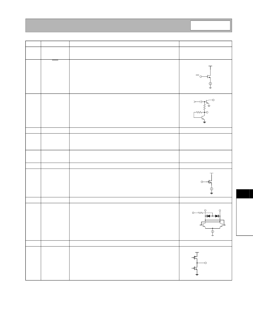
T
Pin
1
Function
GND1
Description
Ground connection for the analog circuits, including TX buffer and out-
put amplifier. Internally connected to die flag. For best performance,
keep traces physically short and connect immediately to ground plane.
Power Down control for all circuitry. When this pin is a logic “l(fā)ow” all cir-
cuits are turned off. When this pin is a logic “high”, all circuits are oper-
ating normally. See electrical parameters for “high” and “l(fā)ow”
thresholds.
Interface Schematic
2
PD
3
TXOUT
Transmitter output. This output is an open collector and requires a pull-
up inductor for bias/matching and a tapped capacitor for matching.
4
5
VCC1
MOD IN
This pin is used to supply bias to the TX buffer amplifier.
AM analog or digital modulation can be imparted to the carrier by an
input to this pin. An external resistor is used to bias the output amplifi-
ers through this pin. The voltage at this pin must not exceed 1.1V.
Higher voltages may damage the device.
This pin is used to supply DC bias to the VCO, crystal oscillator, pre-
scaler, phase detector, and charge pump. An IF bypass capacitor
should be connected directly to this pin and returned to ground.
Digital PLL ground connection.
See pin 3.
6
VCC2
7
8
GND2
VREF P
Bias voltage reference pin for bypassing the prescaler and phase
detector. The bypass capacitor should be of appropriate size to provide
filtering of the reference crystal frequency and be connected directly to
this pin.
9
GND3
RESNTR-
See pin 1.
10
The RESNTR pins are used to supply DC voltage to the VCO, as well
as to tune the center frequency of the VCO. Equal value inductors
should be connected to this pin and pin 11.
11
12
RESNTR+
LOOP FLT
See pin 10.
Output of the charge pump. An RC network from this pin to ground is
used to establish the PLL bandwidth.
V
CC
PD
TX OUT
MOD IN
RF IN
VREFP
V
CC
RESNTR-
RESNTR+
LOOP FLT
4 k
LOOP FLT
V
CC
相關(guān)PDF資料 |
PDF描述 |
|---|---|
| RF2516 | VHF/UHF TRANSMITTER |
| RF2601 | GAIN CONTROLLED IF AMPLIFIER |
| RF2603 | 2.8V PCS UPCONVERTER |
| RF2607 | CDMA/FM RECEIVE AGC AMPLIFIER |
| RF2608 | 887368322 |
相關(guān)代理商/技術(shù)參數(shù) |
參數(shù)描述 |
|---|---|
| RF2514_06 | 制造商:RFMD 制造商全稱:RF Micro Devices 功能描述:VHF/UHF TRANSMITTER |
| RF2514_1 | 制造商:RFMD 制造商全稱:RF Micro Devices 功能描述:VHF/UHF TRANSMITTER |
| RF2514PCBA | 制造商:RFMD 制造商全稱:RF Micro Devices 功能描述:VHF/UHF TRANSMITTER |
| RF2514PCBA-41X | 制造商:RFMD 制造商全稱:RF Micro Devices 功能描述:VHF/UHF TRANSMITTER |
| RF2516 | 制造商:RF Micro Devices Inc 功能描述:IC TXRX 500MHZ QSOP-16 |
發(fā)布緊急采購,3分鐘左右您將得到回復(fù)。