- 您現在的位置:買賣IC網 > PDF目錄373262 > RF25A RF25A for CDMA. and AMPS Applications PDF資料下載
參數資料
| 型號: | RF25A |
| 英文描述: | RF25A for CDMA. and AMPS Applications |
| 中文描述: | RF25A用于CDMA。和AMPS應用 |
| 文件頁數: | 4/17頁 |
| 文件大?。?/td> | 434K |
| 代理商: | RF25A |
RF25A
RxASIC
4
Conexant–Preliminary
.
ProprietaryInformation
1011110A
August4, 2000
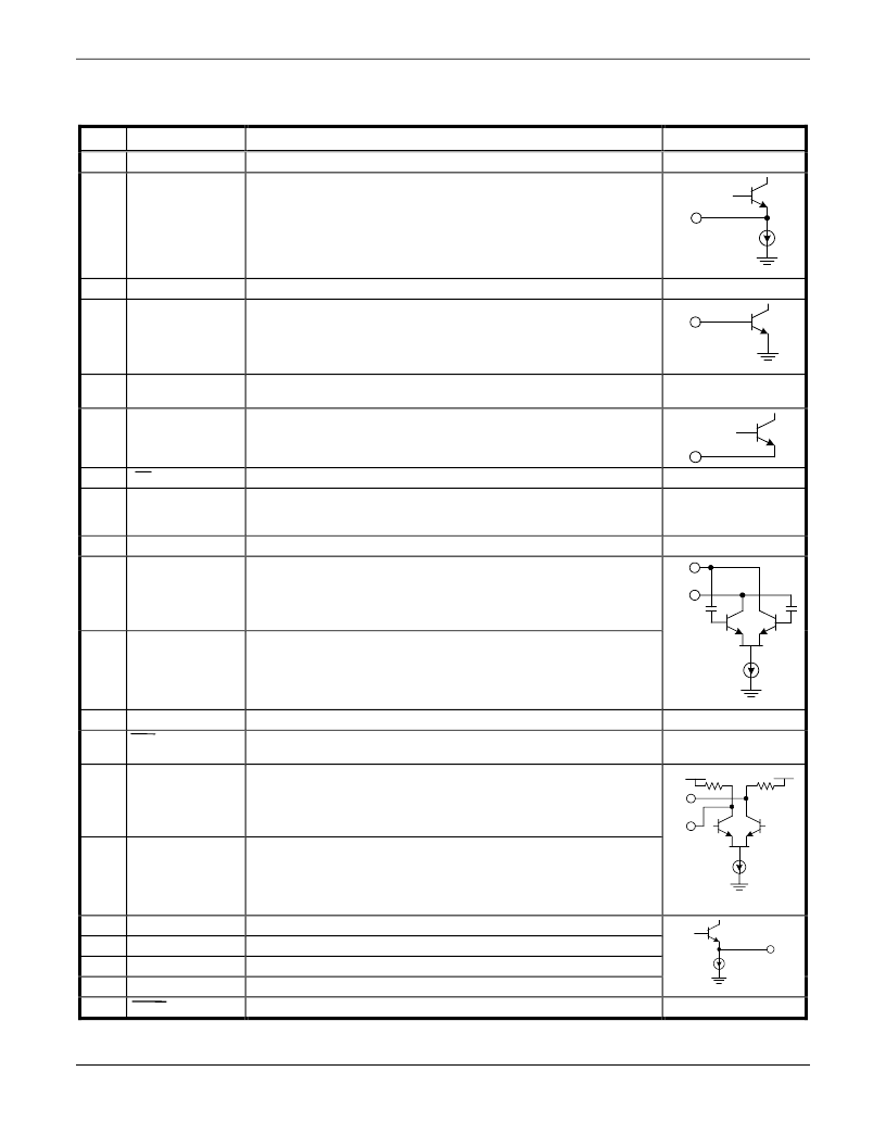
Table1.RF25A PinAssignments andSignalDescriptions (1of3)
Pin#
Name
Description
EquivalentCircuit
1
NC
Noconnection.
2
LNA_DECOUPLE
AnRF bypasscapacitor(1000pF)withveryshorttraceshouldbeconnectedtothispin.
3
NC
Noconnection
4
LNA_IN
TheinputtoLNAneedsexternalmatching.Thematchingnetworkshouldbeplacedasclose
tothispinaspossible.HighQcomponentsarerecommendedtomnimzetheeffectonthe
noisefigure.ADC blockingcapacitorisnecessaryattheinput.
5
VCC_RFBIAS
SupplyvoltagetotheRF bias.AnRF bypasscapacitorshouldbeconnectedfromthepinto
groundwithshorttraces.
6
BIAS_SET
ThispinsetsthecellularRF biascurrent.Typically,a180
resistorisconnectedfromthepin
toground.
7
FM/CDMA
Cellularbandmodeselect:0=AMPS;1=CDMA.
8
VCC_VCO
VoltagesupplypintotheVCObuffer.Abypasscapacitorshouldbeplacedclosetothedevice
frompin8topin9.Thetraceshouldbeshortandconnectedimmediatelytothegroundplane
forbestperformance.
9
GND
GroundreturnfromtheVCObuffer.
10
TANK-
DifferentialtankconnectionforthecellularbandVCO.Careshouldbetakenduringthelayout
oftheexternaltankcircuittopreventparasiticoscillations.
11
TANK+
DifferentialtankconnectionforthecellularbandVCO.Careshouldbetakenduringthelayout
oftheexternaltankcircuittopreventparasiticoscillations.
–
+
12
NC
Noconnection.
13
DIV2/DIV4
SelectsthedivideratiooftheVCOtotheLOportoftheI/Qdemodulator:0=divideby2,
1=divideby40.
14
PLL+
DifferentialbufferedVCOoutput
15
PLL-
DifferentialbufferedVCOoutput
–
+
Vcc
Vcc
16
I+
Ichanneldifferentialoutput.
17
I-
Ichanneldifferentialoutput.
18
Q+
Qchanneldifferentialoutput.
19
Q-
Qchanneldifferentialoutput.
20
SLEEP
Activatessleepmode:0=sleep;1=enable
相關PDF資料 |
PDF描述 |
|---|---|
| RF25H | Analog IC |
| RF25H-LGA | Upconverter |
| RF25H-TQFP | Upconverter |
| RF2679 | Analog IC |
| RF2701 | Quadrature Demodulator |
相關代理商/技術參數 |
參數描述 |
|---|---|
| RF25CCT52AR68K | 制造商:KOA 制造商全稱:KOA Speer Electronics, Inc. 功能描述:coat-insulated fusing resistors (constant current fusing type) |
| RF25CR27J | 功能描述:金屬膜電阻器 - 透孔 FLAMEPROOF FUSIBLE RoHS:否 制造商:IRC 電阻:63.4 kOhms 容差:1 % 功率額定值:100 mW 電壓額定值:200 V 溫度系數:100 PPM / C 端接類型:Axial 工作溫度范圍: 尺寸:2.3 mm Dia. x 6.4 mm L 封裝:Bulk |
| RF25CT52A100J | 制造商:KOA 制造商全稱:KOA Speer Electronics, Inc. 功能描述:coat-insulated fusing resistor |
| RF25H | 制造商:未知廠家 制造商全稱:未知廠家 功能描述:Analog IC |
| RF25H-LGA | 制造商:未知廠家 制造商全稱:未知廠家 功能描述:Upconverter |
發(fā)布緊急采購,3分鐘左右您將得到回復。