- 您現(xiàn)在的位置:買賣IC網(wǎng) > PDF目錄385769 > RF2919 (RF MICRO DEVICES INC) 433/868/915MHZ ASK/OOK RECEIVER PDF資料下載
參數(shù)資料
| 型號: | RF2919 |
| 廠商: | RF MICRO DEVICES INC |
| 元件分類: | 通信及網(wǎng)絡(luò) |
| 英文描述: | 433/868/915MHZ ASK/OOK RECEIVER |
| 中文描述: | SPECIALTY TELECOM CIRCUIT, PQFP32 |
| 封裝: | PLASTIC, LQFP-32 |
| 文件頁數(shù): | 5/18頁 |
| 文件大小: | 519K |
| 代理商: | RF2919 |
11-147
RF2919
Rev A12 001113
11
T
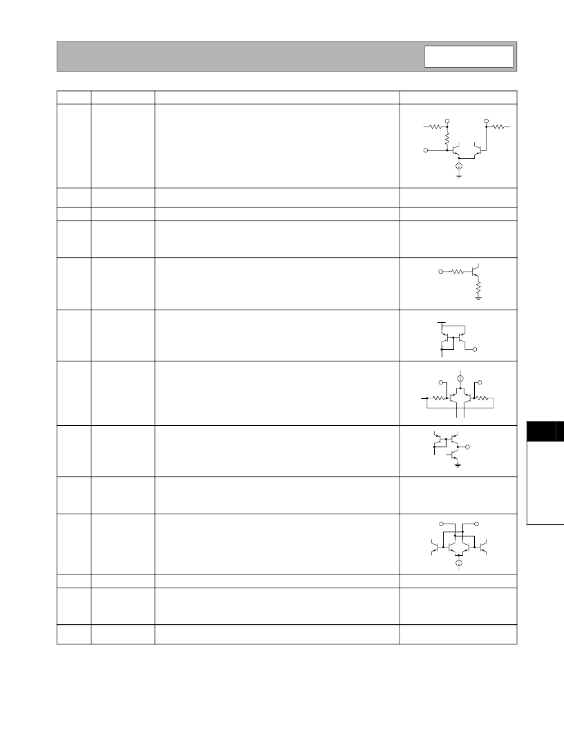
Pin
16
Function
IF2 IN
Description
Inverting input to the 60dB limiting amplifier strip. A 10nF DC blocking
capacitor is required on this input. The IF2 IN input presents a nominal
330
input resistance and interfaces directly to 10.7MHz ceramic fil-
ters.
Interface Schematic
17
IF2 BP+
DC feedback node for the 60dB limiting amplifier strip. A 10nF bypass
capacitor from this pin to ground is required.
See pin 17.
See pin 16.
18
19
IF2 BP-
VCC3
See pin 16.
This pin is used is supply DC bias to the 60dB IF limiting amplifier. An
IF bypass capacitor should be connected directly to this pin and
returned to ground. A 10nF capacitor is recommended for 10.7MHz IF
applications.
This pin is used to mute the data output (DATA OUT). MUTE>2.0V
turns the DATA OUT signal on. MUTE<1.0V turns the DATA OUT signal
off.
20
MUTE
21
RSSI
A DC voltage proportional to the received signal strength is output from
this pin. The output voltage increases with increasing signal strength.
22
DATA IN-
The inverting input of the data comparator. The RSSI is fed to this pin
via a 50k
resistor. This input is available for a data filtering capacitor
that provides noise and 2x IF rejection. The value of the capacitor can
be calculated by C= 1/(2
π
F*50k
) where F is the desired 3dB band-
width.
23
DATA OUT
The data comparator output which contains the modulating data recov-
ered from the RSSI signal. Hysteresis can be added to the comparator
by placing a very large (<1M
) resistor between pins 23 and 24.The
magnitude of the load impedance is intended to be 1M
or greater.
24
DATA IN+
The non-inverting input of the data comparator. The RSSI is fed to this
pin via a 50k
resistor. This input is available for a large filtering capac-
itor such that the modulation signal can be filtered out leaving a DC ref-
erence signal for the comparator.
This port is used to supply DC voltage to the VCO as well as to tune the
center frequency of the VCO. Equal value inductors should be con-
nected to this pin and pin 26.
See pin 22.
25
RESNTR-
26
27
RESNTR+
VCC2
See pin 25.
See pin 25.
This pin is used is supply DC bias to the VCO, prescaler, and PLL. An
IF bypass capacitor should be connected directly to this pin and
returned to ground. A 10nF capacitor is recommended for 10.7MHz IF
applications.
GND4 is the ground shared on chip by the VCO, prescaler, and PLL
electronics.
28
GND4
IF2 IN
330
60 k
60 k
IF2 BP-
IF2 BP+
MUTE
75 k
25 k
V
CC
RSSI
50 k
50 k
DATA IN+
DATA IN-
RSSI
DATA OUT
RESNTR-
RESNTR+
相關(guān)PDF資料 |
PDF描述 |
|---|---|
| RF2926 | UHF DUAL CONVERSION TRANSCEIVER |
| RF2938 | 2.4GHZ SPREAD-SPECTRUM TRANSCEIVER |
| RF2942 | UHF QUADRATURE MODULATOR AND TRANSMITTER |
| RF2945 | 433/868/915MHZ FSK/ASK/OOK TRANSCEIVER |
| RF2958 | 2.4GHz SPREAD-SPECTRUM TRANSCEIVER |
相關(guān)代理商/技術(shù)參數(shù) |
參數(shù)描述 |
|---|---|
| RF2926 | 制造商:RFMD 制造商全稱:RF Micro Devices 功能描述:UHF DUAL CONVERSION TRANSCEIVER |
| RF2926-000 | 制造商:TE Connectivity 功能描述:FEMTOSMDC005F-2 - Tape and Reel |
| RF2926PCBA | 制造商:RFMD 制造商全稱:RF Micro Devices 功能描述:UHF DUAL CONVERSION TRANSCEIVER |
| RF2938 | 制造商:RF Micro Devices Inc 功能描述:Telecommunication IC |
| RF2938TR13 | 制造商:未知廠家 制造商全稱:未知廠家 功能描述:Interface IC |
發(fā)布緊急采購,3分鐘左右您將得到回復(fù)。