- 您現(xiàn)在的位置:買(mǎi)賣(mài)IC網(wǎng) > PDF目錄385769 > RF2958 (RF MICRO DEVICES INC) 2.4GHz SPREAD-SPECTRUM TRANSCEIVER PDF資料下載
參數(shù)資料
| 型號(hào): | RF2958 |
| 廠商: | RF MICRO DEVICES INC |
| 元件分類(lèi): | 無(wú)繩電話/電話 |
| 英文描述: | 2.4GHz SPREAD-SPECTRUM TRANSCEIVER |
| 中文描述: | TELECOM, CELLULAR, RF AND BASEBAND CIRCUIT, QCC32 |
| 封裝: | 5 X 5 MM, QFN-32 |
| 文件頁(yè)數(shù): | 2/20頁(yè) |
| 文件大小: | 235K |
| 代理商: | RF2958 |
第1頁(yè)當(dāng)前第2頁(yè)第3頁(yè)第4頁(yè)第5頁(yè)第6頁(yè)第7頁(yè)第8頁(yè)第9頁(yè)第10頁(yè)第11頁(yè)第12頁(yè)第13頁(yè)第14頁(yè)第15頁(yè)第16頁(yè)第17頁(yè)第18頁(yè)第19頁(yè)第20頁(yè)
11-264
RF2958
Rev A0 050209
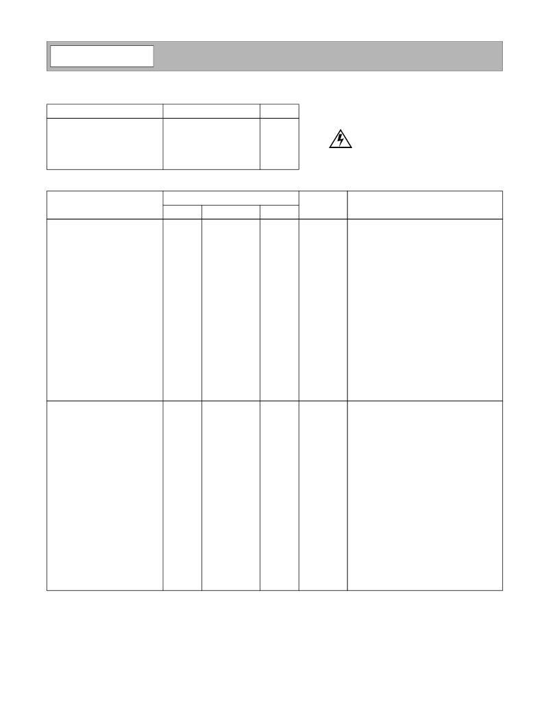
Absolute Maximum Ratings
Parameter
Supply Voltage
Control Voltages
Input RF Level
Operating Ambient Temperature
Storage Temperature
Rating
-0.5 to +3.6
-0.5 to +3.6
+12
-40 to +85
-40 to +150
Unit
V
DC
V
DC
dBm
°C
°C
Parameter
Specification
Typ.
Unit
Condition
Min.
Max.
Receiver LNA/RF
V
CC
=3.0V, T=+25°C, MCLK=44MHz,
unless otherwise specified
RF Frequency Range
IF Frequency Range
Voltage Gain - High
2400
363
32
(20dB
power)
-1
(-13dB
power)
2500
385
38
(26dB
power)
+5
(-7dB
power)
MHz
MHz
dB
374MHz ±11MHz
LNA/mixer voltage gain (Note: into output
impedance). LNA/mixer/SAW filter voltage
gain. LNA GS=1
LNA/mixer voltage gain. LNA GS=0
35
(23dB
power)
+2
(-10dB
power)
4
32
Voltage Gain - Low
dB
Noise Figure - High Gain
Noise Figure - Low Gain
Input IP3 - High Gain
Input IP3 - Low Gain
Input P1dB - High Gain
Input P1dB - Low Gain
Input Return Loss
Output Impedance
Image Rejection
Receiver
IF VGA/Baseband
IF Frequency Range
IF Input Impedance
Voltage Gain - High
dBm
dBm
dBm
dBm
dBm
dBm
dB
dB
-23
+8
-30
-2
10
750
Z
0
=50
30
374
750
MHz
dB
70
V
GC
=1.25V (measured to single-ended out-
put)
V
GC
=1.95V (measured to single-ended out-
put)
For a given RX VGC voltage, the measured
gain should lie within ±3dB of ideal
Measured with a DC step from 1.3V to 1.8V
to 90% final value (within 1dB)
374MHz ±11MHz, relative to gain at
374MHz
Measured into the IF VGA pin.
1dB compression of IF strip.
Measured at input to RF3002 single-ended.
Single-ended.
Voltage Gain - Low
4
dB
Gain Accuracy
±3
dB
Gain Response Time
300
ns
Gain Flatness
-0.25
+0.25
dB
Input Referred Noise
Input V1dB
Output Distortion
Output Voltage
Output V1dB
11
uV
RMS
mV
P-P
%
V
P-P
V
P-P
500
1.0
0.75
1.25
Caution!
ESD sensitive device.
RF Micro Devices believes the furnished information is correct and accurate
at the time of this printing. However, RF Micro Devices reserves the right to
make changes to its products without notice. RF Micro Devices does not
assume responsibility for the use of the described product(s).
Refer to “Handling of PSOP and PSSOP Products” on page 16-15 for
special handling information.
Refer to “Soldering Specifications” on page 16-13 for special solder-
ing information.
相關(guān)PDF資料 |
PDF描述 |
|---|---|
| RF2958PCBA | 2.4GHz SPREAD-SPECTRUM TRANSCEIVER |
| RF2958TR13 | 2.4GHz SPREAD-SPECTRUM TRANSCEIVER |
| RF2968 | BLUETOOTHTM TRANSCEIVER |
| RF3160 | DUAL-BAND GSM/DCS POWER AMP MODULE |
| RF3160PCBA | DUAL-BAND GSM/DCS POWER AMP MODULE |
相關(guān)代理商/技術(shù)參數(shù) |
參數(shù)描述 |
|---|---|
| RF2958PCBA | 制造商:RFMD 制造商全稱:RF Micro Devices 功能描述:2.4GHz SPREAD-SPECTRUM TRANSCEIVER |
| RF2958TR13 | 制造商:RFMD 制造商全稱:RF Micro Devices 功能描述:2.4GHz SPREAD-SPECTRUM TRANSCEIVER |
| RF2959-000 | 制造商:TE Connectivity 功能描述:GAS TUBE 5MM 600V 20% 5KA SMD |
| RF2960-000 | 制造商:TE Connectivity 功能描述:GAS TUBE 8MM 800V 15% 5KA AXIAL |
| RF2961-000 | 制造商:TE Connectivity 功能描述:GAS TUBE 5MM 420V 20% 2.5KA SMD |
發(fā)布緊急采購(gòu),3分鐘左右您將得到回復(fù)。