- 您現(xiàn)在的位置:買賣IC網(wǎng) > PDF目錄376313 > RM2211D883B (Electronic Theatre Controls, Inc.) FSK Demodulator/Tone Decoder PDF資料下載
參數(shù)資料
| 型號(hào): | RM2211D883B |
| 廠商: | Electronic Theatre Controls, Inc. |
| 英文描述: | FSK Demodulator/Tone Decoder |
| 中文描述: | FSK解調(diào)器/音頻解碼器 |
| 文件頁(yè)數(shù): | 6/16頁(yè) |
| 文件大?。?/td> | 135K |
| 代理商: | RM2211D883B |
第1頁(yè)第2頁(yè)第3頁(yè)第4頁(yè)第5頁(yè)當(dāng)前第6頁(yè)第7頁(yè)第8頁(yè)第9頁(yè)第10頁(yè)第11頁(yè)第12頁(yè)第13頁(yè)第14頁(yè)第15頁(yè)第16頁(yè)

PRODUCT SPECIFICATION
RC2211
6
Applications
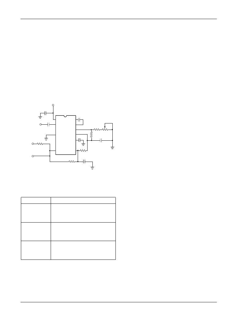
FSK Decoding
Figure 2 shows the basic circuit connection for FSK decod-
ing. With reference to Figures 1 and 2, the functions of
external components are deTned as follows: R
0
and C
0
set
the PLL center frequency, R
1
sets the system bandwidth, and
C
1
sets the loop Tlter time constant and the loop damping
factor. C
F
and R
F
form a one pole post-detection Tlter for the
FSK data output. The resistor R
B
(510 k
W
) from pin 7 to pin
8 introduces positive feedback across FSK comparator to
facilitate rapid transition between output logic states.
Recommended component values for some of the most
commonly used FSK bauds are given in Table 1.
Figure 2. Circuit Connectbn for FSK Decoding
Table 1. Recommended Component Values
for Commonly Used FSK Bands
(see Circuit of Figure 2)
Design Instructions
The circuit of Figure 2 can be tailored for any FSK decoding
application by the choice of Tve key circuit components: R
0
,
R
1
, C
0
, C
1
and C
F
. For a given set of FSK mark and space
frequencies, F
1
and F
2
, these parameters can be calculated as
follows:
FSK Band
300 Baud
F
1
= 1070 Hz
F
2
= 1270 Hz
300 Baud
F
1
= 2025 Hz
F
2
= 2225 Hz
1200 Baud
F
1
= 1200 Hz
F
2
= 2200 Hz
Component Values
C
0
= 0.039
m
F, C
F
= 0.005
m
F
C
1
= 0.01
m
F, R
0
= 18 k
W
R
1
= 100 k
W
C
0
= 0.022
m
F, C
F
= 0.005
m
F
C
1
= 0.0047
m
F, R
0
= 18 k
W
R
1
= 200 k
W
C
0
= 0.027
m
F, C
F
= 0.0022
m
F
C
1
= 0.01
m
F, R
0
= 18 k
W
R
1
= 30 k
W
1
2
3
4
5
6
7
14
13
12
11
10
9
8
RC2211
65-2211-05
C0
VCO
Fine Tune
R0
R
X
5K
R1
C1
0.1
μ
F
R
F
100K
510K
C
F
FSK Data
Output
5.1K
+V
S
0.1
μ
F
0.1
μ
F
+V
S
FSK
Input
R
L
R
B
1.
Calculate PLL center frequency, F
0
2.
Choose a value of timing resistor R
0
to be in the range
of 10 k
W
to 100 k
W
. This choice is arbitrary. The recom-
mended value is R
0
= 20 k
W
. The Tnal value of R
0
ios
normally Tnetuned with the series potentiometer, R
X
.
3.
Calculate value of C
0
from Design Equation No. 1 or
from Typical Performance Characteristics:
C
0
= 1/R
0
F
0
4.
Calculate R
1
to give a
D
f equal to the markspace
deviation:
R
1
= R
0
[F
0
/(F
1
- F
2
)]
5.
Calculate C
1
to set loop damping. (See Design Equation
No. 4)
Normally,
z
1/2 is recommended
Then: C
1
= C
0
/4 for
z
= 1/2
6.
Calculate Data Filter Capacitance, C
F
:
For R
F
= 100 k
W
, R
B
= 510 k
W
, the recommended value
of C
F
is:
Note:
All calculated component values except RO can be
rounded off to the nearest standard value, and R0 can
be varied to fine-tune center frequency through a series
potentiometer, R
X
(see Figure 2).
Design Example
75 Baud FSK demodulator with mark space frequencies of
1110/1170 Hz:
Step 1: Calculate F
0
:
F
0
=(1110+1170)(1/2)= 1140Hz
Step 2: Choose R
0
= 20 k
W
(18 k
W
Txed resistor in series
with 5 k
W
potentiometer)
Step 3: Calculate C
0
from VCO Frequency vs. Timing
Capacitor: C
9
= 0.044
m
F
Step 4: Calculate R
1
: R
1
= R
0
(1140/60) = 380 k
W
Step 5: Calculate C
1
: C
1
= C
0
/4 = 0.011
m
F
Note:
All values except R
0
can be rounded off to nearest
standard value.
fF
0
F
------2
F
2
+
=
C
F
in
m
F
(
)
Baud Rate
-----------3
=
相關(guān)PDF資料 |
PDF描述 |
|---|---|
| RM25 | Avalanche Diodes |
| RM25 | Avalanche Diodes |
| RM26 | Avalanche Diodes |
| RM3183 | Dual ARINC 429 Line Receiver |
| RM3183L | Dual ARINC 429 Line Receiver |
相關(guān)代理商/技術(shù)參數(shù) |
參數(shù)描述 |
|---|---|
| RM221C | 制造商:未知廠家 制造商全稱:未知廠家 功能描述:Logic IC |
| RM221D | 制造商:未知廠家 制造商全稱:未知廠家 功能描述:Logic IC |
| RM221K | 制造商:Ohmite Mfg Co 功能描述: |
| RM222 | 功能描述:SWITCH KEYLOCK 3POS 3CAM PANEL RoHS:是 類別:開(kāi)關(guān) >> 鍵鎖式 系列:Reliant'22 標(biāo)準(zhǔn)包裝:1 系列:P 電路:單刀雙擲 位置數(shù):2 觸點(diǎn)額定電壓:4A @ 125VAC 觸動(dòng)器類型:扁平按鍵 安裝類型:面板安裝 端接類型:導(dǎo)線引線 可拔出鑰匙位置:1 和 2 擺角:90° 其它名稱:Q4871990 |
| RM222-023-211-2000 | 制造商:Airborn Inc 功能描述: |
發(fā)布緊急采購(gòu),3分鐘左右您將得到回復(fù)。