- 您現(xiàn)在的位置:買(mǎi)賣(mài)IC網(wǎng) > PDF目錄376313 > RM3183 (Electronic Theatre Controls, Inc.) Dual ARINC 429 Line Receiver PDF資料下載
參數(shù)資料
| 型號(hào): | RM3183 |
| 廠商: | Electronic Theatre Controls, Inc. |
| 英文描述: | Dual ARINC 429 Line Receiver |
| 中文描述: | 雙的ARINC 429線路接收器 |
| 文件頁(yè)數(shù): | 11/12頁(yè) |
| 文件大?。?/td> | 86K |
| 代理商: | RM3183 |

RM3183
PRODUCT SPECIFICATION
11
Mechanical Dimensions
(continued)
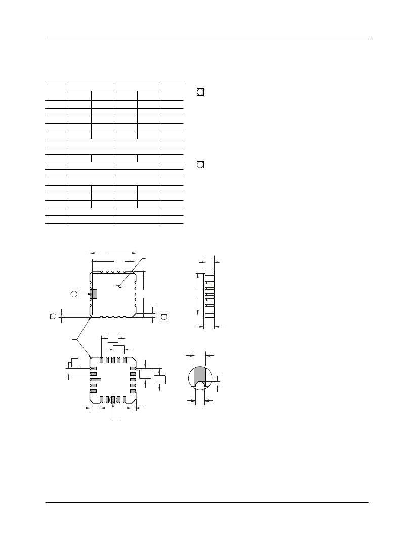
20-Terminal LCC
E
D
D3
A1
A
L2
D2
D1
PLANE 2
PLANE 1
LID
B3
L3
L1
e
4
INDEX
CORNER
DETAIL "A"
DETAIL "A"
(j) X 45
°
(h) X 45
°
3 PLCS
E2
E1
4
E3
B1
1
A
A1
B1
B3
D/E
.060
.050
.022
.006
.342
.100
.088
.028
.022
.358
1.52
1.27
.56
.15
8.69
2.54
2.24
.71
.56
9.09
3, 6
3, 6
2
Symbol
Inches
Min.
Max.
Min.
Max.
Millimeters
Notes
D1/E1
D2/E2
D3/E3
.200 BSC
.100 BSC
—
5.08 BSC
2.54 BSC
—
.050 BSC
.040 REF
.020 REF
.045
.075
.003
1.27 BSC
1.02 REF
.51 REF
1.14
1.91
.08
5
5
20
20
4
4
e
h
j
L1
L2
L3
ND/NE
N
.055
.095
.015
1.40
2.41
.38
5
2, 5
.358
9.09
Notes:
1.
The index feature for terminal 1 identification, optical orientation or
handling purposes, shall be within the shaded index areas shown
on planes 1 and 2. Plane 1, terminal 1 identification may be an
extension of the length of the metallized terminal which shall not be
wider than the B1 dimension.
2.
Unless otherwise specified, a minimum clearance of .015 inch
(0.38mm) shall be maintained between all metallized features (e.g.,
lid, castellations, terminals, thermal pads, etc.).
3.
Dimension "A" controls the overall package thickness. The
maximum "A" dimension is the package height before being solder
dipped.
4.
The corner shape (square, notch, radius, etc.) may vary at the
manufacturer's option, from that shown on the drawing. The index
corner shall be clearly unique.
5.
Dimension "B3" minimum and "L3" minimum and the appropriately
derived castellation length define an unobstructed three
dimensional space traversing all of the ceramic layers in which a
castellation was designed. Dimensions "B3" and "L3" maximum
define the maximum width and depth of the castellation at any point
on its surface. Measurement of these dimensions may be made
prior to solder dripping.
6.
Chip carriers shall be constructed of a minimum of two ceramic
layers.
相關(guān)PDF資料 |
PDF描述 |
|---|---|
| RM3183L | Dual ARINC 429 Line Receiver |
| RM3183S | Dual ARINC 429 Line Receiver |
| RM400HA-34S | Super Fast Recovery Single Diode Module (400 Amperes/1700 Volts) |
| RM4136 | Quad General-Purpose Operational Amplifiers(通用型四運(yùn)放) |
| RM4136FK | QUAD GENERAL-PURPOSE OPERATIONAL AMPLIFIERS |
相關(guān)代理商/技術(shù)參數(shù) |
參數(shù)描述 |
|---|---|
| RM3183CH | 制造商:未知廠家 制造商全稱(chēng):未知廠家 功能描述:Line Receiver |
| RM3183D | 制造商:未知廠家 制造商全稱(chēng):未知廠家 功能描述:Line Receiver |
| RM3183D/883B | 制造商:未知廠家 制造商全稱(chēng):未知廠家 功能描述:Line Receiver |
| RM3183L | 制造商:未知廠家 制造商全稱(chēng):未知廠家 功能描述:Dual ARINC 429 Line Receiver |
| RM3183L/883B | 制造商:未知廠家 制造商全稱(chēng):未知廠家 功能描述:Line Receiver |
發(fā)布緊急采購(gòu),3分鐘左右您將得到回復(fù)。