- 您現(xiàn)在的位置:買賣IC網(wǎng) > PDF目錄192300 > S29PL032J65BFI150 (SPANSION LLC) 2M X 16 FLASH 3V PROM, 65 ns, PBGA56 PDF資料下載
參數(shù)資料
| 型號: | S29PL032J65BFI150 |
| 廠商: | SPANSION LLC |
| 元件分類: | PROM |
| 英文描述: | 2M X 16 FLASH 3V PROM, 65 ns, PBGA56 |
| 封裝: | 7 X 9 MM, LEAD FREE, FBGA-56 |
| 文件頁數(shù): | 11/94頁 |
| 文件大?。?/td> | 949K |
| 代理商: | S29PL032J65BFI150 |
第1頁第2頁第3頁第4頁第5頁第6頁第7頁第8頁第9頁第10頁當前第11頁第12頁第13頁第14頁第15頁第16頁第17頁第18頁第19頁第20頁第21頁第22頁第23頁第24頁第25頁第26頁第27頁第28頁第29頁第30頁第31頁第32頁第33頁第34頁第35頁第36頁第37頁第38頁第39頁第40頁第41頁第42頁第43頁第44頁第45頁第46頁第47頁第48頁第49頁第50頁第51頁第52頁第53頁第54頁第55頁第56頁第57頁第58頁第59頁第60頁第61頁第62頁第63頁第64頁第65頁第66頁第67頁第68頁第69頁第70頁第71頁第72頁第73頁第74頁第75頁第76頁第77頁第78頁第79頁第80頁第81頁第82頁第83頁第84頁第85頁第86頁第87頁第88頁第89頁第90頁第91頁第92頁第93頁第94頁
July 29, 2005 S29PL-J_00_A8
S29PL-J
17
Advance
Information
Device Bus Operations
This section describes the requirements and use of the device bus operations, which are initiated
through the internal command register. The command register itself does not occupy any ad-
dressable memory location. The register is a latch used to store the commands, along with the
address and data information needed to execute the command. The contents of the register
serve as inputs to the internal state machine. The state machine outputs dictate the function of
the device. Table 1 lists the device bus operations, the inputs and control levels they require, and
the resulting output. The following subsections describe each of these operations in further
detail.
Legend: L = Logic Low = VIL, H = Logic High = VIH, VID = 11.5–12.5 V, VHH = 8.5–9.5 V, X = Don’t Care, SA = Sector
Address, AIN = Address In, DIN = Data In, DOUT = Data Out
Notes:
1. The sector protect and sector unprotect functions may also be implemented via programming equipment. See the High
Voltage Sector Protection section.
2. WP#/ACC must be high when writing to upper two and lower two sectors.
Requirements for Reading Array Data
To read array data from the outputs, the system must drive the OE# and appropriate CE# pins
(For PL129J - CE1#/CE2# pins) to VIL. In PL129J, CE1# and CE2# are the power control and
select the lower (CE1#) or upper (CE2#) halves of the device. CE# is the power control. OE# is
the output control and gates array data to the output pins. WE# should remain at VIH.
The internal state machine is set for reading array data upon device power-up, or after a hard-
ware reset. This ensures that no spurious alteration of the memory content occurs during the
power transition. No command is necessary in this mode to obtain array data. Standard micro-
processor read cycles that assert valid addresses on the device address inputs produce valid data
on the device data outputs. Each bank remains enabled for read access until the command reg-
ister contents are altered.
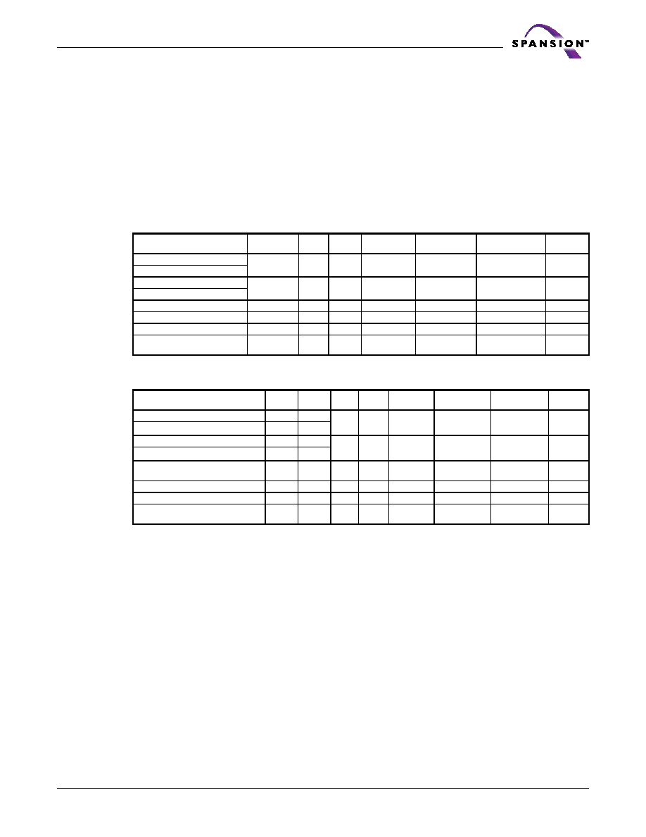
Table 1 PL127J Device Bus Operations
Operation
CE#
OE#
WE#
RESET#
WP#/ACC
Addresses
(Amax–A0)
DQ15–
DQ0
Read
LL
H
X
AIN
DOUT
Write
LH
L
H
X (Note 2)AIN
DIN
Standby
VIO±0.3 V
X
VIO ±0.3 V
High-Z
Output Disable
L
H
X
High-Z
Reset
X
L
X
High-Z
Temporary Sector Unprotect
(High Voltage)
XX
X
VID
XAIN
DIN
Table 2 PL129J Device Bus Operations
Operation
CE1#
CE2#
OE#
WE#
RESET#
WP#/ACC
Addresses
(A21–A0)
DQ15–
DQ0
Read
L
H
LH
H
X
AIN
DOUT
HL
Write
L
H
HL
H
X
AIN
DIN
HL
Standby
VIO±
0.3 V
VIO ±
0.3 V
XX
VIO ±
0.3 V
XX
High-Z
Output Disable
L
H
X
High-Z
Reset
X
L
X
High-Z
Temporary Sector Unprotect
(High Voltage)
XX
X
VID
XAIN
DIN
相關PDF資料 |
PDF描述 |
|---|---|
| S29PL127J70BFI000 | 8M X 16 FLASH 3V PROM, 70 ns, PBGA80 |
| S29XS064R0PBHW010 | 4M X 16 FLASH 1.8V PROM, 80 ns, PBGA44 |
| S2C3R-1-12-H | 4000 MHz - 12000 MHz RF/MICROWAVE SGL POLE DOUBLE THROW SWITCH, 2 dB INSERTION LOSS |
| S2C5R-1-12-RC | 4000 MHz - 18000 MHz RF/MICROWAVE SGL POLE DOUBLE THROW SWITCH, 2.8 dB INSERTION LOSS |
| S2H3R-1H | 10 MHz - 1000 MHz RF/MICROWAVE SGL POLE DOUBLE THROW SWITCH, 1.2 dB INSERTION LOSS |
相關代理商/技術參數(shù) |
參數(shù)描述 |
|---|---|
| S29PL032J70BAI120 | 功能描述:閃存 32Mb 3V 70ns Parallel NOR 閃存 RoHS:否 制造商:ON Semiconductor 數(shù)據(jù)總線寬度:1 bit 存儲類型:Flash 存儲容量:2 MB 結構:256 K x 8 定時類型: 接口類型:SPI 訪問時間: 電源電壓-最大:3.6 V 電源電壓-最小:2.3 V 最大工作電流:15 mA 工作溫度:- 40 C to + 85 C 安裝風格:SMD/SMT 封裝 / 箱體: 封裝:Reel |
| S29PL032J70BAI122 | 功能描述:閃存 32MB 閃存 3V 70ns Parallel NOR 閃存 RoHS:否 制造商:ON Semiconductor 數(shù)據(jù)總線寬度:1 bit 存儲類型:Flash 存儲容量:2 MB 結構:256 K x 8 定時類型: 接口類型:SPI 訪問時間: 電源電壓-最大:3.6 V 電源電壓-最小:2.3 V 最大工作電流:15 mA 工作溫度:- 40 C to + 85 C 安裝風格:SMD/SMT 封裝 / 箱體: 封裝:Reel |
| S29PL032J70BAW120 | 功能描述:閃存 32MB 閃存 3V 70ns Parallel NOR 閃存 RoHS:否 制造商:ON Semiconductor 數(shù)據(jù)總線寬度:1 bit 存儲類型:Flash 存儲容量:2 MB 結構:256 K x 8 定時類型: 接口類型:SPI 訪問時間: 電源電壓-最大:3.6 V 電源電壓-最小:2.3 V 最大工作電流:15 mA 工作溫度:- 40 C to + 85 C 安裝風格:SMD/SMT 封裝 / 箱體: 封裝:Reel |
| S29PL032J70BFI120 | 功能描述:閃存 32Mb 3V 70ns Parallel NOR 閃存 RoHS:否 制造商:ON Semiconductor 數(shù)據(jù)總線寬度:1 bit 存儲類型:Flash 存儲容量:2 MB 結構:256 K x 8 定時類型: 接口類型:SPI 訪問時間: 電源電壓-最大:3.6 V 電源電壓-最小:2.3 V 最大工作電流:15 mA 工作溫度:- 40 C to + 85 C 安裝風格:SMD/SMT 封裝 / 箱體: 封裝:Reel |
| S29PL032J70BFI120(E) | 制造商:Spansion 功能描述:Cut Tape |
發(fā)布緊急采購,3分鐘左右您將得到回復。