- 您現(xiàn)在的位置:買賣IC網(wǎng) > PDF目錄368612 > S5N8950 (SAMSUNG SEMICONDUCTOR CO. LTD.) G.dmt ADSL Transceiver for CO and CPE PDF資料下載
參數(shù)資料
| 型號: | S5N8950 |
| 廠商: | SAMSUNG SEMICONDUCTOR CO. LTD. |
| 英文描述: | G.dmt ADSL Transceiver for CO and CPE |
| 中文描述: | G.dmt寬帶收發(fā)器對CO和CPE |
| 文件頁數(shù): | 9/19頁 |
| 文件大小: | 203K |
| 代理商: | S5N8950 |
S5N8950
G.dmt ADSL Transceiver for CO and CPE
CONFIDENTIAL
Preliminary Information ( Rev 1.2 )
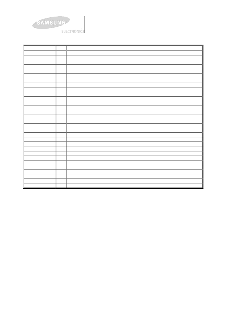
Pad
I/O
I
I
OZ
O
O
I
I
I
I
I
B
Description
PHTIC
PHTICD
PHTOT4
PHOB4
PHOB2
PHIC
PHICD
PHICU
PHICD
PHIS
PHTBCT4
5V tolerant for 3.3 V interface LVCMOS level input buffer
5V tolerant for 3.3 V interface LVCMOS level input buffer with pull-down register.
5V tolerant for 3.3 V interface tri-state output buffer driving 4 mA
3.3 V LVCMOS normal output buffer driving 4 mA
3.3 V LVCMOS normal output buffer driving 2 mA
3.3 V interface LVCMOS level input buffer
3.3 V interface LVCMOS level input buffer with pull-down register.
3.3 V interface LVCMOS level input buffer with pull-up resister
3.3 V interface LVCMOS level input buffer with pull-down resister
3.3 V interface LVCMOS Schmitt-trigger level input buffer
3.3 V interface 5 V tolerant LVCMOS level tri-state bi-directional buffer
driving 4 mA
3.3 V interface 5 V tolerant LVCMOS level tri-state bi-directional buffer
driving 6 mA medium slew rate control
3.3 V interface 5 V tolerant LVCMOS level tri-state bi-directional buffer
driving 6 mA medium slew rate control with pull-down register.
Analog normal output pad for 1.8 V interface
with resister 50 Ohm and separated bulk bias
Oscillator cell with enable and feedback resistor.
Power, 1.8 V total with separate bulk bias
Ground, 1.8 V total with separate bulk bias
Ground, 1.8 V bulk bias
VDD for 1.8 V internal power
VSS for 1.8 V internal power
VDD for 3.3 V output driver power
VSS for 3.3 V output driver power
VDD for 3.3 V pre- driver power
VSS for 3.3 V pre- driver power
VDD for 3.3 V output driver and pre- driver power
VSS for 3.3 V output driver and pre- driver power
PHTBCT6SM
B
PHTBCDT6SM
B
POAR50_ABB
O
PHSOSCM26
VDD1T_ABB
VSS1T_ABB
VBB1_ABB
VDD1I
VSS1I
VDD3O
VSS3O
VDD3P
VSS3P
VDD3OP
VSS3OP
I/O
I
I
I
I
I
I
I
I
I
I
I
Table 2: Pad description
相關(guān)PDF資料 |
PDF描述 |
|---|---|
| S5N8951 | G.dmt ADSL Analog Front End IC |
| S5N8951X | G.dmt ADSL Analog Front End IC |
| S5N8952 | ADSL Transceiver for NIC |
| S5N8952X | ADSL Transceiver for NIC |
| S5T8610 | DIGITAL CLP MODEM WITH ADPCM CODEC |
相關(guān)代理商/技術(shù)參數(shù) |
參數(shù)描述 |
|---|---|
| S5N8951 | 制造商:SAMSUNG 制造商全稱:Samsung semiconductor 功能描述:G.dmt ADSL Analog Front End IC |
| S5N8951X | 制造商:SAMSUNG 制造商全稱:Samsung semiconductor 功能描述:G.dmt ADSL Analog Front End IC |
| S5N8952 | 制造商:SAMSUNG 制造商全稱:Samsung semiconductor 功能描述:ADSL Transceiver for NIC |
| S5N8952X | 制造商:SAMSUNG 制造商全稱:Samsung semiconductor 功能描述:ADSL Transceiver for NIC |
| S5-P | 制造商:TURCK Inc 功能描述:Relay, Socket, Releco S5-P, 3 Pole, 11 Contact, PCB Mount, R4518 |
發(fā)布緊急采購,3分鐘左右您將得到回復(fù)。