- 您現(xiàn)在的位置:買賣IC網(wǎng) > PDF目錄368613 > S6C0670 (SAMSUNG SEMICONDUCTOR CO. LTD.) 8 BIT 384 / 402 CHANNEL TFT-LCD SOURCE DRIVER PDF資料下載
參數(shù)資料
| 型號: | S6C0670 |
| 廠商: | SAMSUNG SEMICONDUCTOR CO. LTD. |
| 英文描述: | 8 BIT 384 / 402 CHANNEL TFT-LCD SOURCE DRIVER |
| 中文描述: | 8位402分之384通道TFT - LCD的源驅(qū)動 |
| 文件頁數(shù): | 7/32頁 |
| 文件大?。?/td> | 332K |
| 代理商: | S6C0670 |
第1頁第2頁第3頁第4頁第5頁第6頁當(dāng)前第7頁第8頁第9頁第10頁第11頁第12頁第13頁第14頁第15頁第16頁第17頁第18頁第19頁第20頁第21頁第22頁第23頁第24頁第25頁第26頁第27頁第28頁第29頁第30頁第31頁第32頁
8 BIT 384 / 402 CHANNEL TFT-LCD SOURCE DRIVER
S6C0670
7
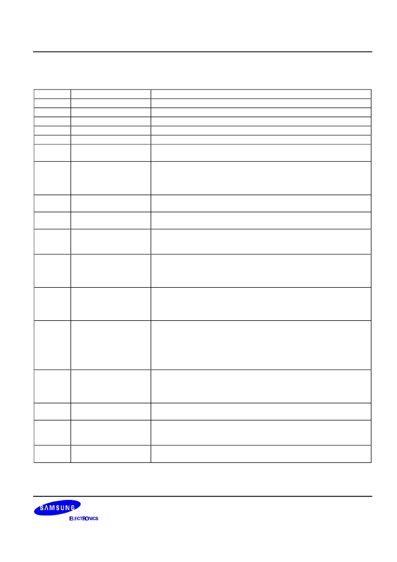
PIN DESCRIPTIONS
Symbol
VDD1
VDD2
VSS1
VSS2
Y1 - Y402
D0<0:7>
- D5<0:7>
Pin Name
Logic power supply
Driver power supply
Logic ground
Driver ground
Driver outputs
Description
2.5 - 3.6 V
8.0 - 15.0 V
Ground (0 V)
Ground (0 V)
The D/A converted 256 gray-scale analog voltage is output.
The display data is input with a width of 48 bits,
gray-scale data (8 bits) by 6 dots (R,G,B) DX0: LSB, DX7: MSB
This pin controls the direction of shift register in cascade connection.
The shift direction of the shift registers is as follows.
SHL = H: DIO1 input, Y1
→
Y402, DIO2 output
SHL = L: DIO2 input, Y402
→
Y1, DIO1 output
SHL = H: Used as the start pulse input pin.
SHL = L: Used as the start pulse output pin.
SHL = H: Used as the start pulse output pin.
SHL = L: Used as the start pulse input pin.
DATPOL1,2 = L: Display data is not inverted
DATPOL1 = H: Display data of D0<0:7> - D2<0:7> is inverted
DATPOL2 = H: Display data of D3<0:7> - D5<0:7> is inverted
POL = H: The reference voltage for odd number outputs are VGMA9 –
VGMA16 and those for even number outputs are VGMA1 – VGMA8.
POL = L: The reference voltage for odd number outputs are VGMA1 –
VGMA8 and those for even number outputs are VGMA9 – VGMA16.
Refer to the shift register's shift clock input. When DEC is Low, the
display data is loaded to the data register at the rising edge of
CLK2.When DEC is High, the display data is loaded to the data register
at the rising and falling edge of CLK2.
Latches the contents of the data register at rising edge and transfers
them to the D/A converter. Also, after CLK1 input, clears the internal
shift register contents. After 1 pulse input on start, operates normally.
CLK1 input timing refers to the "Relationships between CLK1 start pulse
(DIO1, DIO2) and blanking period" of the switching characteristic
waveform. Outputs the G/S data at falling edge.
Input the gamma corrected power supplies from external source.
VDD2 > VGMA1 > VGMA2 >
……
> VGMA15 > VGMA16 > VSS2
Keep gray-scale power supply unchanged during the gray-scale
voltage output.
SELT = L: 384 Output (Y193 - Y210 are disabled), SELT = H: 402
Output
DEC = L: Single Edge, the display data is loaded to the data register at
the rising edge of CLK2. DEC = H: Double Edge, the display data is
loaded to the data register at the rising and falling edge of CLK2.
TEST = L: Normal operation mode
TEST = H: Test mode (OP AMP CUT-OFF, Rpd = 10k
)
Display data input
SHL
Shift direction control
input
DIO1
Start pulse input/output
DIO2
Start pulse input/output
DATPOL1
DATPOL2
Data inversion input
POL
Polarity input
CLK2
Shift clock input
CLK1
Latch input
VGMA1
–
VGMA16
Gamma corrected power
supplies
SELT
Output selection input
DEC
Double edge selection
input
TEST
Test input
相關(guān)PDF資料 |
PDF描述 |
|---|---|
| S6C0671 | 8 BIT 384 CHANNEL TFT-LCD SOURCE DRIVER |
| S6C0672 | 6 BIT 384 CHANNEL TFT-LCD SOURCE DRIVER |
| S6C0676 | 6 BIT 480 CHANNEL TFT-LCD SOURCE DRIVER |
| S6C0678 | 6 BIT 420 CHANNEL TFT-LCD SOURCE DRIVER |
| S6C0679 | 6 BIT 420 CHANNEL RSDS TFT-LCD SOURCE DRIVER |
相關(guān)代理商/技術(shù)參數(shù) |
參數(shù)描述 |
|---|---|
| S6C0671 | 制造商:SAMSUNG 制造商全稱:Samsung semiconductor 功能描述:8 BIT 384 CHANNEL TFT-LCD SOURCE DRIVER |
| S6C0672 | 制造商:SAMSUNG 制造商全稱:Samsung semiconductor 功能描述:6 BIT 384 CHANNEL TFT-LCD SOURCE DRIVER |
| S6C0676 | 制造商:SAMSUNG 制造商全稱:Samsung semiconductor 功能描述:6 BIT 480 CHANNEL TFT-LCD SOURCE DRIVER |
| S6C0678 | 制造商:SAMSUNG 制造商全稱:Samsung semiconductor 功能描述:6 BIT 420 CHANNEL TFT-LCD SOURCE DRIVER |
| S6C0679 | 制造商:SAMSUNG 制造商全稱:Samsung semiconductor 功能描述:6 BIT 420 CHANNEL RSDS TFT-LCD SOURCE DRIVER |
發(fā)布緊急采購,3分鐘左右您將得到回復(fù)。