- 您現(xiàn)在的位置:買賣IC網(wǎng) > PDF目錄231009 > S71PL032J80BAW052 (SPANSION LLC) SPECIALTY MEMORY CIRCUIT, PBGA56 PDF資料下載
參數(shù)資料
| 型號: | S71PL032J80BAW052 |
| 廠商: | SPANSION LLC |
| 元件分類: | 存儲器 |
| 英文描述: | SPECIALTY MEMORY CIRCUIT, PBGA56 |
| 封裝: | 7 X 9 MM, 1.20 MM HEIGHT, FBGA-56 |
| 文件頁數(shù): | 143/188頁 |
| 文件大小: | 5078K |
| 代理商: | S71PL032J80BAW052 |
第1頁第2頁第3頁第4頁第5頁第6頁第7頁第8頁第9頁第10頁第11頁第12頁第13頁第14頁第15頁第16頁第17頁第18頁第19頁第20頁第21頁第22頁第23頁第24頁第25頁第26頁第27頁第28頁第29頁第30頁第31頁第32頁第33頁第34頁第35頁第36頁第37頁第38頁第39頁第40頁第41頁第42頁第43頁第44頁第45頁第46頁第47頁第48頁第49頁第50頁第51頁第52頁第53頁第54頁第55頁第56頁第57頁第58頁第59頁第60頁第61頁第62頁第63頁第64頁第65頁第66頁第67頁第68頁第69頁第70頁第71頁第72頁第73頁第74頁第75頁第76頁第77頁第78頁第79頁第80頁第81頁第82頁第83頁第84頁第85頁第86頁第87頁第88頁第89頁第90頁第91頁第92頁第93頁第94頁第95頁第96頁第97頁第98頁第99頁第100頁第101頁第102頁第103頁第104頁第105頁第106頁第107頁第108頁第109頁第110頁第111頁第112頁第113頁第114頁第115頁第116頁第117頁第118頁第119頁第120頁第121頁第122頁第123頁第124頁第125頁第126頁第127頁第128頁第129頁第130頁第131頁第132頁第133頁第134頁第135頁第136頁第137頁第138頁第139頁第140頁第141頁第142頁當(dāng)前第143頁第144頁第145頁第146頁第147頁第148頁第149頁第150頁第151頁第152頁第153頁第154頁第155頁第156頁第157頁第158頁第159頁第160頁第161頁第162頁第163頁第164頁第165頁第166頁第167頁第168頁第169頁第170頁第171頁第172頁第173頁第174頁第175頁第176頁第177頁第178頁第179頁第180頁第181頁第182頁第183頁第184頁第185頁第186頁第187頁第188頁
May 21, 2004 S29PL127_064_032J_00_A1
S29PL127J/S29PL064J/S29PL032J for MCP
57
Prelimin ary
Hardware Data Protection
The command sequence requirement of unlock cycles for programming or erasing
provides data protection against inadvertent writes. In addition, the following
hardware data protection measures prevent accidental erasure or programming,
which might otherwise be caused by spurious system level signals during VCC
power-up and power-down transitions, or from system noise.
Low VCC Write Inhibit
When VCC is less than VLKO, the device does not accept any write cycles. This pro-
tects data during VCC power-up and power-down. The command register and all
internal program/erase circuits are disabled, and the device resets to the read
mode. Subsequent writes are ignored until VCC is greater than VLKO. The system
must provide the proper signals to the control pins to prevent unintentional writes
when VCC is greater than VLKO.
Write Pulse “Glitch” Protection
Noise pulses of less than 3 ns (typical) on OE#, CE#, or WE# do not initiate a
write cycle.
Logical Inhibit
Write cycles are inhibited by holding any one of OE# = VIL, CE# = VIH or WE# =
VIH. To initiate a write cycle, CE# and WE# must be a logical zero while OE# is a
logical one.
Power-Up Write Inhibit
If WE# = CE# = VIL and OE# = VIH during power up, the device does not accept
commands on the rising edge of WE#. The internal state machine is automatically
reset to the read mode on power-up.
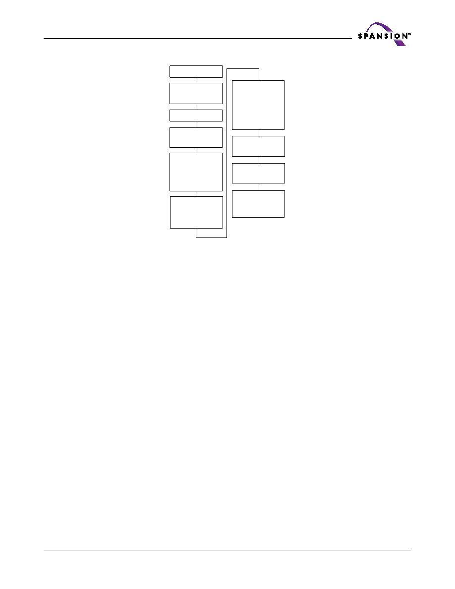
Figure 3. SecSi Sector Protect Verify
Write 60h to
any address
Write 40h to SecSi
Sector address
with A6 = 0,
A1 = 1, A0 = 0
START
RESET# =
VIH or VID
Wait 1
s
Read from SecSi
Sector address
with A6 = 0,
A1 = 1, A0 = 0
If data = 00h,
SecSi Sector is
unprotected.
If data = 01h,
SecSi Sector is
protected.
Remove VIH or VID
from RESET#
Write reset
command
SecSi Sector
Protect Verify
complete
相關(guān)PDF資料 |
PDF描述 |
|---|---|
| S71PL032J80BAW074 | SPECIALTY MEMORY CIRCUIT, PBGA56 |
| S71PL032JA0BAW074 | SPECIALTY MEMORY CIRCUIT, PBGA56 |
| S71PL032JA0BFW0F4 | SPECIALTY MEMORY CIRCUIT, PBGA56 |
| S29JL032H60TAI023 | 2M X 16 FLASH 3V PROM, 60 ns, PDSO48 |
| S29AL016D70BAI022 | 1M X 16 FLASH 3V PROM, 70 ns, PBGA48 |
相關(guān)代理商/技術(shù)參數(shù) |
參數(shù)描述 |
|---|---|
| S71PL032J80BAW0Z0 | 制造商:SPANSION 制造商全稱:SPANSION 功能描述:Based MCPs |
| S71PL032J80BAW0Z2 | 制造商:SPANSION 制造商全稱:SPANSION 功能描述:Based MCPs |
| S71PL032J80BAW0Z3 | 制造商:SPANSION 制造商全稱:SPANSION 功能描述:Based MCPs |
| S71PL032J80BAW9Z0 | 制造商:SPANSION 制造商全稱:SPANSION 功能描述:Based MCPs |
| S71PL032J80BAW9Z2 | 制造商:SPANSION 制造商全稱:SPANSION 功能描述:Based MCPs |
發(fā)布緊急采購,3分鐘左右您將得到回復(fù)。