- 您現(xiàn)在的位置:買賣IC網(wǎng) > PDF目錄385812 > SA56600-42 (NXP Semiconductors N.V.) System reset for lithium battery backup PDF資料下載
參數(shù)資料
| 型號: | SA56600-42 |
| 廠商: | NXP Semiconductors N.V. |
| 英文描述: | System reset for lithium battery backup |
| 中文描述: | 系統(tǒng)復(fù)位備用鋰電池 |
| 文件頁數(shù): | 8/12頁 |
| 文件大小: | 141K |
| 代理商: | SA56600-42 |
Philips Semiconductors
Product data
SA56600-42
System reset for lithium battery back-up
2001 Jun 19
8
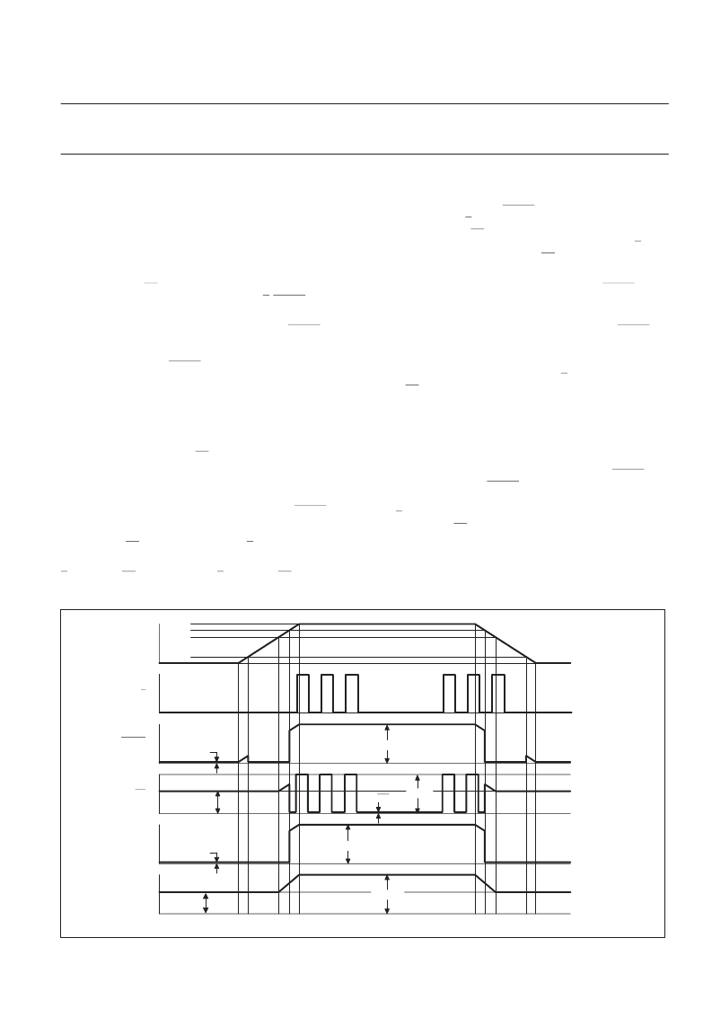
Timing diagram
The Timing Diagram shown in Figure 15 depicts the operation of the
SA56600-42 in its intended application, with a 3.0 V Lithium battery
serving as a backup power source for external SRAM circuitry (see
the Simplified system diagram, Figure 1). Letters indicate events
along the Time axis.
A:
At ‘A’, the V
CC
primary power source is off. As a result of the
backup battery, the CS and V
OUT
outputs are almost up to the
Lithium battery potential (V
B
). All other outputs (Y, RESET, and CS)
are at or very near ground potential.
B - C:
At ‘B’, the V
CC
voltage begins to rise. Also the RESET
voltage initially rises but then abruptly returns to a LOW state at ‘C’.
when the V
CC
voltage reaches the level which activates the internal
bias circuitry and asserts RESET to a logic LOW. This occurs at
approximately 0.8 volts.
D - E:
At ‘D’ the internal 3.3 V detection circuit is activated when
V
CC
voltage rises to 3.3 V. The circuit causes the PNP series pass
switching transistor in the output to activate, connecting the main
power supply voltage (V
CC
) to the output. This causes the Lithium
battery to be automatically disconnected from V
OUT
by back-biasing
the Schottky diode. As a result, CS and V
OUT
begin to rise with V
CC
.
E:
At ‘E’, V
CC
has risen to the upper detection threshold (V
S
plus
hysteresis) as sensed by the device’s internal 4.2 V detection circuit.
This event signals that the output voltage is adequate to support full
operation of the associated external computer circuitry. RESET goes
HIGH, allowing the microprocessor circuitry to operate.
Simultaneously, CS also goes HIGH, signaling the SRAM to start
receiving data. CS goes LOW as a result of Y simultaneously being
at a LOW state.
Y controls the CS output. As long as Y is LOW, the CS output is
enabled.
F:
As V
CC
continues to rise, RESET, CS, and V
OUT
also continue to
rise. Just before ‘F’, Y is asserted HIGH by the microprocessing
circuitry. This causes CS to change from a LOW state to a HIGH
state. Following ‘F’ the microprocessing circuitry is signaling Y
through repetitive cycles. This causes CS to also cycle, but has no
effect on the battery circuit.
G:
At ‘G’, the V
CC
voltage begins to fall. As a result RESET, CS,
and V
CC
fall.
H:
When the V
CC
voltage falls to V
S
(4.2 V) it is detected by the
internal 4.2 V detector circuit. The detector circuit forces RESET and
CS LOW, deselecting the SRAM and stopping data storage and
retrieval. The PNP series pass switching transistor disconnects the
primary input source voltage from the output, transferring the SRAM
to the backup battery. In addition, because Y is already at a LOW
state, CS rises abruptly close to V
S
followed by a continued fall to
V
B
(Lithium battery potential), following V
CC
.
J:
At ‘J’, V
OUT
has also fallen with V
CC
to a level that is now
dictated by the Lithium battery potential. The Lithium battery is now
maintaining the V
OUT
voltage to preserve the SRAM data.
K - L:
As the V
CC
voltage falls to a level which no longer allows the
internal bias circuitry to remain active, the assertion of RESET can
no longer be maintained. RESET rises slightly, then falls to ground
as V
CC
falls to ground.
M:
Y is asserted HIGH again by the microprocessor, but because
V
CC
is below V
S
, CS remains HIGH and CS remains LOW,
preventing the SRAM from being selected.
TIME
A
B C
D E F
G H
J
K
0
0
0
L
0
0
0
V
RSH
V
O1, O2
V
CSH
V
CSL
V
O3, O4
V
CSL
≤
V
B
V
RSL
V
OUT
CS
CS
RESET
Y
V
CC
V
S
V
B
SL01341
V
OPL
V
CSH
Figure 15. Timing diagram.
相關(guān)PDF資料 |
PDF描述 |
|---|---|
| SA56614-42 | CMOS system reset |
| SA568A | Ceramic Multilayer Capacitor; Capacitor Type:General Purpose; Capacitance:2200pF; Capacitance Tolerance: 10%; Voltage Rating:100VDC; Capacitor Dielectric Material:Multilayer Ceramic; Package/Case:0603; Termination:SMD RoHS Compliant: Yes |
| SA568AD | 150MHz phase-locked loop |
| SA568AN | 150MHz phase-locked loop |
| SA577N | Unity gain level programmable low power compandor |
相關(guān)代理商/技術(shù)參數(shù) |
參數(shù)描述 |
|---|---|
| SA56606-20 | 制造商:PHILIPS 制造商全稱:NXP Semiconductors 功能描述:CMOS system reset |
| SA56606-20GW | 制造商:PHILIPS 制造商全稱:NXP Semiconductors 功能描述:CMOS system reset |
| SA56606-27 | 制造商:PHILIPS 制造商全稱:NXP Semiconductors 功能描述:CMOS system reset |
| SA56606-27GW | 制造商:PHILIPS 制造商全稱:NXP Semiconductors 功能描述:CMOS system reset |
| SA56606-28 | 制造商:PHILIPS 制造商全稱:NXP Semiconductors 功能描述:CMOS system reset |
發(fā)布緊急采購,3分鐘左右您將得到回復(fù)。