- 您現(xiàn)在的位置:買賣IC網(wǎng) > PDF目錄385813 > SAA7110 (NXP SEMICONDUCTORS) Digital Multistandard Colour Decoder(數(shù)字多標準彩色譯碼器) PDF資料下載
參數(shù)資料
| 型號: | SAA7110 |
| 廠商: | NXP SEMICONDUCTORS |
| 元件分類: | 顏色信號轉(zhuǎn)換 |
| 英文描述: | Digital Multistandard Colour Decoder(數(shù)字多標準彩色譯碼器) |
| 中文描述: | COLOR SIGNAL DECODER, PQCC68 |
| 封裝: | PLASTIC, MO-047AC, SOT-188-2, LCC-68 |
| 文件頁數(shù): | 6/76頁 |
| 文件大小: | 416K |
| 代理商: | SAA7110 |
第1頁第2頁第3頁第4頁第5頁當前第6頁第7頁第8頁第9頁第10頁第11頁第12頁第13頁第14頁第15頁第16頁第17頁第18頁第19頁第20頁第21頁第22頁第23頁第24頁第25頁第26頁第27頁第28頁第29頁第30頁第31頁第32頁第33頁第34頁第35頁第36頁第37頁第38頁第39頁第40頁第41頁第42頁第43頁第44頁第45頁第46頁第47頁第48頁第49頁第50頁第51頁第52頁第53頁第54頁第55頁第56頁第57頁第58頁第59頁第60頁第61頁第62頁第63頁第64頁第65頁第66頁第67頁第68頁第69頁第70頁第71頁第72頁第73頁第74頁第75頁第76頁
1995 Oct 18
6
Philips Semiconductors
Product specification
One Chip Front-end 1 (OCF1)
SAA7110; SAA7110A
8
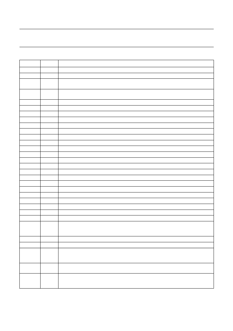
PINNING
SYMBOL
PIN
DESCRIPTION
SP
AP
RTCO
1
2
3
test pin input; (shift pin) connect to ground for normal operation
test pin input; (action pin) connect to ground for normal operation
Real Time Control Output. This pin is used to fit serially the increments of the HPLL and
FSC-PLL and information of the PAL or SECAM sequence.
I
2
C-bus slave address select input. LOW: slave address = 9CH for write, 9DH for read;
HIGH = 9DH for write, 9FH for read.
I
2
C-bus serial data input/output
I
2
C-bus serial clock input
reserved pin; do not connect
reserved pin; do not connect
reserved pin; do not connect
ground for analog input 4
analog input 42
supply voltage (+5 V) for analog input 4
analog input 41
ground for analog input 3
analog input 32
supply voltage (+5 V) for analog input 3
analog input 31
ground for analog input 2
analog input 22
supply voltage (+5 V) for analog input 2
analog input 21
substrate ground
analog test output; do not connect
supply voltage (+5 V) for internal CGC (Clock Generation Circuit)
ground for internal CGC
Line Frequency Control output; this is the analog clock control signal driving the external
CGC. The frequency is a multiple of the actual line frequency (nominally 7.375/6.13636 MHz).
The signal has a triangular form with 4-bit accuracy.
supply voltage (+5 V)
ground
Line-Locked Clock input/output (CGCE = 1, output; CGCE = 0, input). This is the system
clock, its frequency is 1888
×
f
h
for 50 Hz/625 lines per field systems and 1560
×
f
h
for
60 Hz/525 lines per field systems; or variable input clock up to 32 MHz in input mode.
Line-Locked Clock
1
2
output; f
LLC2
= 0.5
×
f
LLC
(CGCE = 1, output; CGCE = 0, high
impedance).
Clock reference input/output (CGCE = 1, output; CGCE = 0, input). This is a clock qualifier
signal distributed by the internal or an external clock generator circuit (CGC). Using CREF all
interfaces on the YUV-bus are able to generate a bus timing with identical phase.
SA
4
SDA
SCL
i.c.
i.c.
i.c.
V
SSA4
AI42
V
DDA4
AI41
V
SSA3
AI32
V
DDA3
AI31
V
SSA2
AI22
V
DDA2
AI21
V
SS(S)
AOUT
V
DDA0
V
SSA0
LFCO
5
6
7
8
9
10
11
12
13
14
15
16
17
18
19
20
21
22
23
24
25
26
V
DD
V
SS
LLC
27
28
29
LLC2
30
CREF
31
相關(guān)PDF資料 |
PDF描述 |
|---|---|
| SAA7111 | Video Input Processor VIP |
| SAA7120H | Digital video encoder |
| SAA7152 | Digital Video Comb Filter DCF |
| SAA7184 | Digital Video Encoders DENC2-M6 |
| SAA7187 | Digital video encoder (DENC2-SQ)(數(shù)字視頻編碼器) |
相關(guān)代理商/技術(shù)參數(shù) |
參數(shù)描述 |
|---|---|
| SAA7110/7110A | 制造商:未知廠家 制造商全稱:未知廠家 功能描述:One Chip Frontend 1 (OCF1) Product Specification |
| SAA7110A | 制造商:PHILIPS 制造商全稱:NXP Semiconductors 功能描述:One Chip Front-end 1 OCF1 |
| SAA7110AWP/00 | 制造商:NXP Semiconductors 功能描述: |
| SAA7111 | 制造商:PHILIPS 制造商全稱:NXP Semiconductors 功能描述:Video Input Processor VIP |
| SAA7111A | 制造商:PHILIPS 制造商全稱:NXP Semiconductors 功能描述:Enhanced Video Input Processor EVIP |
發(fā)布緊急采購,3分鐘左右您將得到回復。