- 您現(xiàn)在的位置:買賣IC網(wǎng) > PDF目錄372116 > SAA7740 (NXP Semiconductors N.V.) Digital Audio Processing IC DAPIC PDF資料下載
參數(shù)資料
| 型號: | SAA7740 |
| 廠商: | NXP Semiconductors N.V. |
| 英文描述: | Digital Audio Processing IC DAPIC |
| 中文描述: | 數(shù)字音頻處理集成電路賈皮奇 |
| 文件頁數(shù): | 4/28頁 |
| 文件大小: | 142K |
| 代理商: | SAA7740 |
第1頁第2頁第3頁當(dāng)前第4頁第5頁第6頁第7頁第8頁第9頁第10頁第11頁第12頁第13頁第14頁第15頁第16頁第17頁第18頁第19頁第20頁第21頁第22頁第23頁第24頁第25頁第26頁第27頁第28頁
1997 May 30
4
Philips Semiconductors
Product specification
Digital Audio Processing IC (DAPIC)
SAA7740H
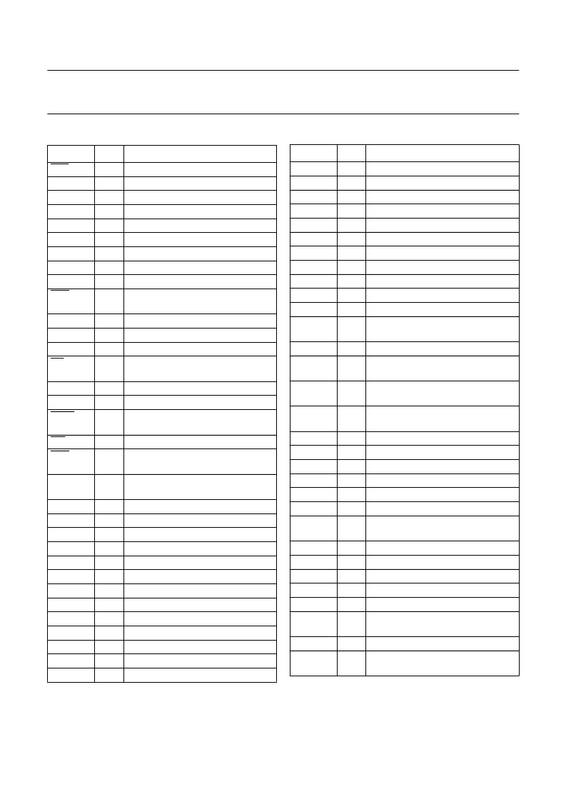
PINNING
SYMBOL
PIN
DESCRIPTION
RST
SCL
SDA
MUTE
n.c.
n.c.
V
DD
V
DD
V
SS
CAS
1
2
3
4
5
6
7
8
9
10
reset input (active LOW)
serial clock input (I
2
C-bus)
serial data input/output (I
2
C-bus)
mute input (active HIGH)
not connected
not connected
supply voltage
supply voltage
ground supply
column address strobe (DRAM)
(active LOW)
input/output data bus line 0 (DRAM)
input/output data bus line 1 (DRAM)
ground supply
output buffer enable (DRAM)
(active LOW)
input/output data bus line 2 (DRAM)
input/output data bus line 3 (DRAM)
second column address strobe
(active LOW)
write enable (DRAM; active LOW)
row address strobe (DRAM;
active LOW)
inverse MSB address line output
(DRAM)
address line output 8 (DRAM)
address line output 7 (DRAM)
address line output 6 (DRAM)
address line output 5 (DRAM)
ground supply
supply voltage
address line output 4 (DRAM)
address line output 3 (DRAM)
address line output 2 (DRAM)
address line output 1 (DRAM)
address line output 0 (DRAM)
supply voltage
address latch strobe output (SRAM)
D0
D1
V
SS
OE
11
12
13
14
D2
D3
CAS2
15
16
17
WE
RAS
18
19
A8B
20
A8
A7
A6
A5
V
SS
V
DD
A4
A3
A2
A1
A0
V
DD
MUX
21
22
23
24
25
26
27
28
29
30
31
32
33
DO1D
DO2D
DOWS
DOBCK
V
DD
n.c.
V
SS
DI1D
DI2D
DIWS
DIBCK
TSTCLK
34
35
36
37
38
39
40
41
42
43
44
45
digital audio output 1 (I
2
S-bus)
digital audio output 2 (I
2
S-bus)
digital audio input word select
digital audio input serial bit clock
supply voltage
not connected
ground supply
digital audio input 1 (I
2
S-bus)
digital audio input 2 (I
2
S-bus)
digital audio input word select
digital audio input serial bit clock
clock input for test mode
(should be tied LOW)
ground supply
test pin input 1
(should be tied LOW)
test pin input 2
(should be tied LOW)
test pin input 3
(should be tied LOW)
ground supply
address select input 1 (I
2
C-bus)
address select input 2 (I
2
C-bus)
supply voltage
supply voltage
ground supply
clock or crystal input
V
SS
TST1
46
47
TST2
48
TST3
49
V
SS
AS1
AS2
V
DD
V
DD
V
SS
CLK1/
XTAL1
n.c.
n.c.
XTAL2
V
DDX
V
SSX
SCCLK
50
51
52
53
54
55
56
57
58
59
60
61
62
not connected
not connected
crystal output 2
crystal supply voltage
crystal ground supply
scan test clock input
(should be tied LOW)
clock signal output
mode select input
(should be tied HIGH)
CLKO
ALL
63
64
SYMBOL
PIN
DESCRIPTION
相關(guān)PDF資料 |
PDF描述 |
|---|---|
| SAA7740H | Digital Audio Processing IC DAPIC |
| SAA7780 | ThunderBird Q3DE PCI Audio Accelerator(雷鳥 Q3DE PCI音頻加速器) |
| SAA7785 | ThunderBird Avenger(TM) PCI Audio Accelerator(雷鳥Avenger(TM)PCI音頻加速器) |
| SAA7811HL | Single-chip DVD-ROM(單片DVD-ROM) |
| SAA7818HL | DVD and CD playback IC |
相關(guān)代理商/技術(shù)參數(shù) |
參數(shù)描述 |
|---|---|
| SAA7740H | 制造商:PHILIPS 制造商全稱:NXP Semiconductors 功能描述:Digital Audio Processing IC DAPIC |
| SAA7750-N1D | 制造商:PHILIPS 制造商全稱:NXP Semiconductors 功能描述:Generic device for portable multimedia applications |
| SAA7780 | 制造商:PHILIPS 制造商全稱:NXP Semiconductors 功能描述:ThunderBird Q3D PCI Audio Accelerator |
| SAA7785 | 制造商:PHILIPS 制造商全稱:NXP Semiconductors 功能描述:ThunderBird Avenger PCI Audio Accelerator |
| SAA7806 | 制造商:PHILIPS 制造商全稱:NXP Semiconductors 功能描述:One chip automotive CD audio device |
發(fā)布緊急采購,3分鐘左右您將得到回復(fù)。