- 您現(xiàn)在的位置:買賣IC網 > PDF目錄376341 > SCM6343YJ15AR (MOTOROLA INC) 256K x 15 Bit 3.3 V Asynchronous Fast Static RAM PDF資料下載
MCM6343
6
MOTOROLA FAST SRAM
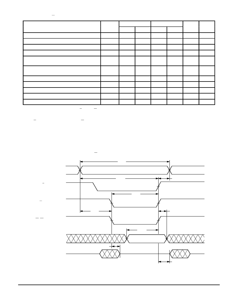
WRITE CYCLE 1
(W Controlled; See Notes 1, 2, and 3)
Parameter
Symbol
b l
MCM6343–12
MCM6343–15
U i
Unit
Notes
Min
Max
Min
Max
Write Cycle Time
tAVAV
tAVWL
tAVWH
tAVWH
tWLWH
tWLEH
12
—
15
—
ns
4
Address Setup Time
0
—
0
—
ns
Address Valid to End of Write
10
—
12
—
ns
Address Valid to End of Write (G High)
9
—
10
—
ns
Write Pulse Width
10
—
12
—
ns
Write Pulse Width (G High)
tWLWH
tWLEH
9
—
10
—
ns
Data Valid to End of Write
tDVWH
tWHDX
tWLQZ
tWHQX
tWHAX
6
—
7
—
ns
Data Hold Time
0
—
0
—
ns
Write Low to Data High–Z
0
6
0
7
ns
5, 6, 7
Write High to Output Active
3
—
3
—
ns
5, 6, 7
Write Recovery Time
0
—
0
—
ns
NOTES:
1. A write occurs during the overlap of E low and W low.
2. Product sensitivities to noise require proper grounding and decoupling of power supplies as well as minimization or elimination of bus
contention conditions during read and write cycles.
3. If G goes low coincident with or after W goes low, the output will remain in a high–impedance state.
4. All write cycle timings are referenced from the last valid address to the first transitioning address.
5. This parameter is sampled and not 100% tested.
6. Transition is measured
±
200 mV from steady–state voltage.
7. At any given voltage and temperature, tWLQZ max < tWHQX min both for a given device and from device to device.
DATA VALID
tDVWH
tAVWL
tAVWH
tAVAV
tWHAX
tWLWH
tWHDX
tWLQZ
tWHQX
HIGH–Z
HIGH–Z
A (ADDRESS)
W (WRITE ENABLE)
E (CHIP ENABLE)
Q (DATA OUT)
D (DATA IN)
tWLEH
LB, UB (BYTE ENABLE)
WRITE CYCLE 1
(W Controlled; See Notes 1, 2, and 3)
相關PDF資料 |
PDF描述 |
|---|---|
| SCM6946 | 512Kx8 Bit Static Random Access Memory(512Kx8位靜態(tài)RAM) |
| SCM69C232 | 4Kx64 Content Adressable Memory(4Kx64內容可尋址存儲器) |
| SCM69C233 | 4K x 64 Content Addressable Memory(4K x 64內容可尋址存儲器) |
| SCM69C432 | 16K x 64Content Addressable Memory(16K x 64內容可尋址存儲器) |
| SCM69C433 | A Flexible Content-Addressable Memory (16K x 64 CAM)(1M內容可尋址存儲器) |
相關代理商/技術參數(shù) |
參數(shù)描述 |
|---|---|
| SCM6378XLDN | 制造商:Sumitomo Wiring Systems LTD 功能描述: |
| SCM-64S | 制造商:Pan Pacific 功能描述: |
| SCM69C233TQ15 | 制造商:Rochester Electronics LLC 功能描述:- Bulk |
| SCM69C433 | 制造商:MOTOROLA 制造商全稱:Motorola, Inc 功能描述:16K x 64 CAM |
| SCM69C433TQ15 | 制造商:MOTOROLA 制造商全稱:Motorola, Inc 功能描述:16K x 64 CAM |
發(fā)布緊急采購,3分鐘左右您將得到回復。