- 您現(xiàn)在的位置:買賣IC網(wǎng) > PDF目錄372130 > SCN2651 (NXP Semiconductors N.V.) Programmable communications interface PCI PDF資料下載
參數(shù)資料
| 型號(hào): | SCN2651 |
| 廠商: | NXP Semiconductors N.V. |
| 英文描述: | Programmable communications interface PCI |
| 中文描述: | 可編程通信接口的PCI |
| 文件頁(yè)數(shù): | 3/15頁(yè) |
| 文件大小: | 118K |
| 代理商: | SCN2651 |
第1頁(yè)第2頁(yè)當(dāng)前第3頁(yè)第4頁(yè)第5頁(yè)第6頁(yè)第7頁(yè)第8頁(yè)第9頁(yè)第10頁(yè)第11頁(yè)第12頁(yè)第13頁(yè)第14頁(yè)第15頁(yè)

Philips Semiconductors
Product specification
SCN2651
Programmable communications interface (PCI)
1994 Apr 27
3
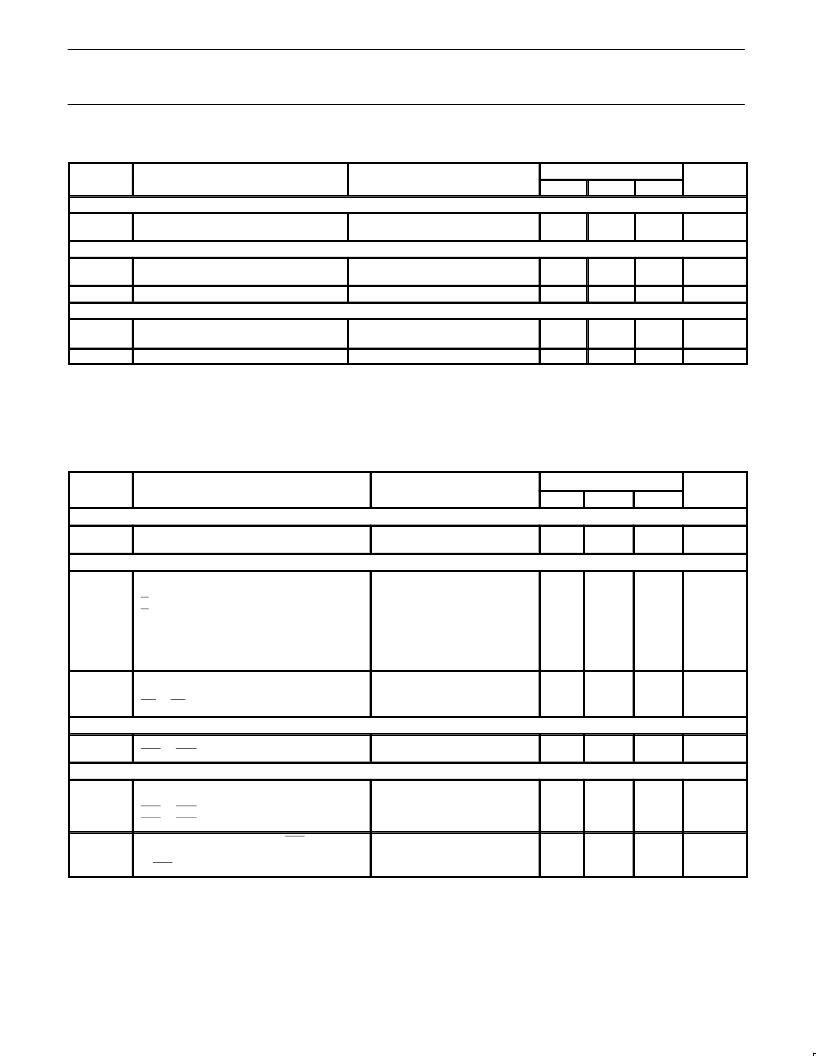
DC ELECTRICAL CHARACTERISTICS
1, 2, 3
SYMBOL
PARAMETER
TEST CONDITIONS
LIMITS
Typ
UNIT
Min
Max
Input voltage
V
IL
V
IH
Output voltage
V
OL
V
OH
I
IL
3-State output leakage current
I
LH
I
LL
Data bus low
I
CC
Power supply current
NOTES:
1. Parameters are valid over operating temperature range unless otherwise specified. See ordering code table for applicable temperature
range and operating supply range.
2. All voltage measurements are referenced to ground. All time measurements are at the 50% level for inputs (except t
BRH
and t
BRL
) and at
0.8V and 2.0V for outputs. Input levels for testing are 0.45V and 2.4V.
3. Typical values are at +25
°
C, typical supply voltages and typical processing parameters.
Low
High
2.0
0.8
V
V
Low
High
Input leakage current
I
OL
= 1.6mA
I
OH
= -100
μ
A
V
IN
= 0 to 5.25V
2.4
-10
0.4
V
V
μ
A
10
Data bus high
V
O
= 4.0V
V
O
= 0.45V
-10
-10
10
10
150
μ
A
μ
A
mA
AC ELECTRICAL CHARACTERISTICS
1, 2, 3
LIMITS
Typ
SYMBOL
Pulse width
t
RES
t
CE
Set-up and hold time
t
AS
t
AH
t
CS
t
CH
t
DS
t
DH
t
RXS
t
RXH
PARAMETER
TEST CONDITIONS
Min
Max
UNIT
Reset
Chip enable
1000
300
ns
ns
Address setup
Address hold
R/W control setup
R/W control hold
Data setup for write
Data hold for write
RX data setup
RX data hold
20
20
20
20
225
0
300
350
ns
ns
ns
ns
ns
ns
ns
ns
t
DD
t
DF
t
CED
Data delay time for read
Data bus floating time for read
CE to CE delay
C
L
= 100pF
C
L
= 100pF
700
250
150
ns
ns
ns
Input clock frequency
f
f
BRG
Clock width
t
BRH5
t
BRL5
t
t
R/TH
t
TXD
t
TCS
Baud rate generator
TxC or RxC
1.0
dc
5.0688
5.0738
1.0
MHz
MHz
Baud rate high
Baud rate low
TxC or RxC high
TxC or RxC low
70
70
500
500
ns
ns
ns
ns
TxD delay from falling edge of TxC
Skew between TxD changing and falling
edge
of TxC output
4
C
L
= 100pF
C
L
= 100pF
0
650
ns
ns
NOTES:
1. Parameters are valid over operating temperature range unless otherwise specified. See ordering code table for applicable temperature
range and operating supply range.
2. All voltage measurements are referenced to ground. All time measurements are at the 50% level for inputs (except t
BRH
and t
BRL
) and at
0.8V and 2.0V for outputs. Input levels for testing are 0.45V and 2.4V.
3. Typical values are at +25
°
C, typical supply voltages and typical processing parameters.
4. Parameter applies when internal transmitter clock is used.
5. Under test conditions of 5.0688MHz, f
BRG
, t
BRH
, and t
BRL
measured at V
IH
and V
IL
respectively.
6. t
R/T
and t
R/TL
shown for all modes except local loopback. For local loopback mode f
R/T
= 0.7MHz and t
R/TL
= 700ns min.
相關(guān)PDF資料 |
PDF描述 |
|---|---|
| SCN2651CC1N28 | Programmable communications interface PCI |
| SCN2652 | Multi-protocol communications controller MPCC |
| SCN2652AC2A44 | NT Series Toggle Switch, 1 pole, 3 position, Solder terminal, Locking Lever |
| SCN2652AC2N40 | Multi-protocol communications controller MPCC |
| SCN68652 | Multi-protocol communications controller MPCC |
相關(guān)代理商/技術(shù)參數(shù) |
參數(shù)描述 |
|---|---|
| SCN2651C1N28 | 制造商:North American Philips Discrete Products Div 功能描述:1 CHANNEL(S), 1M bps, SERIAL COMM CONTROLLER, PDIP28 |
| SCN2651CC1I28 | 制造商:NXP Semiconductors 功能描述:IC,COMMUNICATIONS INTERFACE,MOS,DIP,28PIN,CERAMIC |
| SCN2651CC1N28 | 制造商:NXP Semiconductors 功能描述:COMMUNICATIONS INTERFACE, 28 Pin, Plastic, DIP |
| SCN2652 | 制造商:PHILIPS 制造商全稱:NXP Semiconductors 功能描述:Multi-protocol communications controller MPCC |
| SCN2652AC1I40 | 制造商:North American Philips Discrete Products Div 功能描述:COMMUNICATIONS INTERFACE, 40 Pin, Ceramic, DIP |
發(fā)布緊急采購(gòu),3分鐘左右您將得到回復(fù)。