- 您現(xiàn)在的位置:買賣IC網(wǎng) > PDF目錄372130 > SCN68681E1A44 (NXP SEMICONDUCTORS) Dual asynchronous receiver/transmitter DUART PDF資料下載
參數(shù)資料
| 型號: | SCN68681E1A44 |
| 廠商: | NXP SEMICONDUCTORS |
| 元件分類: | 微控制器/微處理器 |
| 英文描述: | Dual asynchronous receiver/transmitter DUART |
| 中文描述: | 2 CHANNEL(S), 1M bps, SERIAL COMM CONTROLLER, PQCC44 |
| 封裝: | PLASTIC, MS-018, LCC-44 |
| 文件頁數(shù): | 11/28頁 |
| 文件大小: | 187K |
| 代理商: | SCN68681E1A44 |
第1頁第2頁第3頁第4頁第5頁第6頁第7頁第8頁第9頁第10頁當(dāng)前第11頁第12頁第13頁第14頁第15頁第16頁第17頁第18頁第19頁第20頁第21頁第22頁第23頁第24頁第25頁第26頁第27頁第28頁

Philips Semiconductors
Product specification
SCN68681
Dual asynchronous receiver/transmitter (DUART)
1998 Sep 04
11
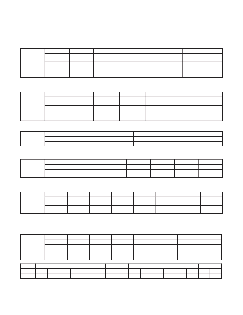
Table 2.
Register Bit Formats
BIT 7
RxRTS
CONTROL
BIT 6
RxINT
SELECT
BIT 5
ERROR
MODE*
BIT 4 BIT 3
BIT 2
PARITY
TYPE
BIT 1 BIT 0
BITS PER
CHARACTER
00 = 5
01 = 6
10 = 7
11 = 8
MR1A
MR1B
PARITY MODE
0 = No
1 = Yes
0 = RxRDY
1 = FFULL
0 = Char
1 = Block
00 = With Parity
01 = Force Parity
10 = No Parity
11 = Multidrop Mode
0 = Even
1 = Odd
NOTE:
*In block error mode, block error conditions must be cleared by using the error reset command (command 4x) or a receiver reset.
BIT 7 BIT 6
BIT 5
TxRTS
CONTROL
BIT 4
CTS
BIT 3 BIT 2 BIT 1 BIT 0
MR2A
MR2B
CHANNEL MODE
ENABLE Tx
STOP BIT LENGTH*
00 = Normal
01 = Auto-Echo
10 = Local loop
11 = Remote loop
0 = No
1 = Yes
0 = No
1 = Yes
0 = 0.563
1 = 0.625
2 = 0.688
3 = 0.750
4 = 0.813
5 = 0.875
6 = 0.938
7 = 1.000
8 = 1.563
9 = 1.625
A = 1.688
B = 1.750
C = 1.813
D = 1.875
E = 1.938
F = 2.000
NOTE:
*Add 0.5 to values shown for 0 - 7 if channel is programmed for 5 bits/char.
CSRA
CSRB
BIT 7 BIT 6 BIT 5 BIT 4
RECEIVER CLOCK SELECT
See Text
BIT 3 BIT 2 BIT 1 BIT 0
TRANSMITTER CLOCK SELECT
See Text
NOTE:
* See Table 6 for BRG Test frequencies in this data sheet, and “Extended baud rates for SCN2681, SCN68681, SCC2691, SCC2692,
SCC68681 and SCC2698B” in application notes elsewhere in this publication
BIT 7
BIT 6 BIT 5 BIT 4
MISCELLANEOUS COMMANDS
See Text
BIT 3
BIT 2
BIT 1
BIT 0
CRA
CRB
DISABLE Tx
0 = No
1 = Yes
ENABLE Tx
0 = No
1 = Yes
DISABLE Rx
0 = No
1 = Yes
ENABLE Rx
0 = No
1 = Yes
Not used –
should be 0
NOTE:
*Access to the upper four bits of the command register should be separated by three (3) edges of the X1 clock. A disabled transmitter cannot
be loaded.
BIT 7
BIT 6
FRAMING
ERROR*
0 = No
1 = Yes
BIT 5
PARITY
ERROR*
0 = No
1 = Yes
BIT 4
BIT 3
BIT 2
BIT 1
BIT 0
SRA
SRB
RECEIVED
BREAK*
0 = No
1 = Yes
OVERRUN
ERROR
0 = No
1 = Yes
TxEMT
TxRDY
FFULL
RxRDY
0 = No
1 = Yes
0 = No
1 = Yes
0 = No
1 = Yes
0 = No
1 = Yes
NOTE:
*These status bits are appended to the corresponding data character in the receive FIFO. A read of the status provides these bits (7:5) from the
top of the FIFO together with bits (4:0). These bits are cleared by a “reset error status” command. In character mode they are discarded when
the corresponding data character is read from the FIFO. In block error mode, block error conditions must be cleared by using the error reset
command (command 4x) or a receiver reset.
BIT 7
OP7
BIT 6
OP6
BIT 5
OP5
BIT 4
OP4
BIT 3 BIT 2
OP3
00 = OPR[3]
01 = C/T OUTPUT
10 = TxCB(1x)
11 = RxCB(1x)
BIT 1 BIT 0
OP2
00 = OPR[2]
01 = TxCA(16x)
10 = TxCA(1x)
11 = RxCA(1x)
OPCR
0 = OPR[7]
1 = TxRDYB
0 = OPR[6]
1 = TxRDYA
0 = OPR[5]
1 = RxRDY/
FFULLB
0 = OPR[4]
1 = RxRDY/
FFULLA
OPR
OPR bit
OP pin
NOTE:
The level at the OP pin is the inverse of the bit in the OPR register.
BIT 7
BIT 6
BIT 5
BIT 4
BIT 3
BIT 2
BIT 1
BIT 0
0
1
1
0
0
1
1
0
0
1
1
0
0
1
1
0
0
1
1
0
0
1
1
0
0
1
1
0
0
1
1
0
相關(guān)PDF資料 |
PDF描述 |
|---|---|
| SCN68681 | Dual universal asynchronous receiver/transmitter (DUART)(雙通用異步接收器/傳送器) |
| SCN68681E1F40 | Dual asynchronous receiver/transmitter DUART |
| SCN68681E1N40 | Dual asynchronous receiver/transmitter DUART |
| SCN68681C1A44 | RES 16K OHM 1/16W 0.1% 0402 SMD |
| SCN8039H | SINGLE-CHIP 8-BIT MICROCONTROLLER |
相關(guān)代理商/技術(shù)參數(shù) |
參數(shù)描述 |
|---|---|
| SCN68681E1F40 | 制造商:PHILIPS 制造商全稱:NXP Semiconductors 功能描述:Dual asynchronous receiver/transmitter DUART |
| SCN68681E1N40 | 制造商:PHILIPS 制造商全稱:NXP Semiconductors 功能描述:Dual asynchronous receiver/transmitter DUART |
| SCN-800 | 制造商:MEANWELL 制造商全稱:Mean Well Enterprises Co., Ltd. 功能描述:800W Single Output With Parallel Function |
| SCN-800-12 | 制造商:ASTRODYNE 制造商全稱:Astrodyne Corporation 功能描述:800W With Parallel Function |
| SCN-800-15 | 制造商:ASTRODYNE 制造商全稱:Astrodyne Corporation 功能描述:800W With Parallel Function |
發(fā)布緊急采購,3分鐘左右您將得到回復(fù)。