- 您現(xiàn)在的位置:買賣IC網(wǎng) > PDF目錄376345 > SG1526 (Microsemi Corporation) REGULATING PULSE WIDTH MODULATOR PDF資料下載
參數(shù)資料
| 型號: | SG1526 |
| 廠商: | Microsemi Corporation |
| 英文描述: | REGULATING PULSE WIDTH MODULATOR |
| 中文描述: | 調(diào)控脈寬調(diào)制器 |
| 文件頁數(shù): | 7/9頁 |
| 文件大?。?/td> | 182K |
| 代理商: | SG1526 |

4/90 Rev 1.1 2/94
Copyright
1994
L
IN
F
IN
ITY
Microelectronics Inc.
11861 Western Avenue
∞
∞
Garden Grove, CA 92841
(714) 898-8121
∞
FAX: (714) 893-2570
7
SG1526/SG2526/SG3526
APPLICATION INFORMATION
(continued)
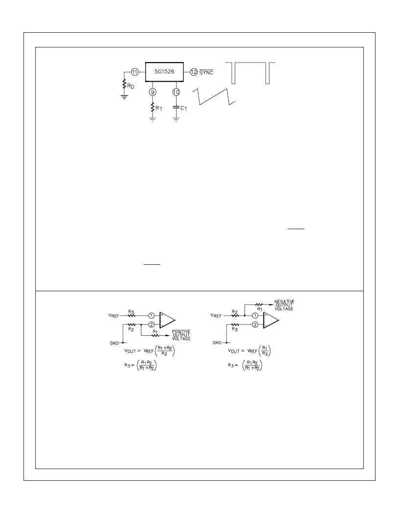
The oscillator is programmed for frequency and deadtime with three components: R
, C
, and R
. Two waveforms are
generated: a sawtooth waveform at pin 10 for pulse width modulation, and a logic clock at pin 12. The following procedure
is recommended for choosing timing values:
1. With R
= 0
(pin 11 shorted to ground) select values for R
and C
from Figure 7 to give the desired oscillator period.
Remember that the frequency at each driver output is half the oscillator frequency, and the frequency at the +V
C
terminal
is the same as the oscillator frequency.
2. If more dead time is required, select a larger value of R
D
using Figure 6 as a guide. At 40kHz dead time increases by
400nSec/ohm.
3. Increasing the dead time will cause the oscillator frequency to decrease slightly. Go back and decrease the value of R
T
slightly to bring the frequency back to the nominal design value.
The SG1526 can be synchronized to an external logic clock by programming the oscillator to free-run at a frequency 10% slower
than the sync frequency. A periodic LOW logic pulse approximately 0.5μSec wide at the SYNC pin will then lock the oscillator
to the external frequency.
Multiple devices can be synchronized together by programming one master unit for the desired frequency, and then sharing
its sawtooth and clock waveforms with the slave units. All C
terminals are connected to the C
pin of the master, and all SYNC
terminals are likewise connected to the SYNC pin of the master. Slave R
terminals should not be left open nor should they
be tied to the +5V reference; at least 50K should be connected to each pin. Slave R
D
terminals may be either left open or
grounded.
OSCILLATOR
FIGURE 21 - OSCILLATOR CONNECTIONS AND WAVEFORMS
The error amplifier is a transconductance design, with an output impedance of 2 megohms and an effective output capacitance
of 100 pF. Since all voltage gain takes place at the output pin, the open-loop gain can be shaped with shunt reactance to ground.
For unity gain stability the amplifier requires an additional external 100 pF to ground, resulting in an open-loop pole at 400 Hz.
The input connections to the error amplifier are determined by the polarity of the switching supply output voltage. For positive
supplies, the common-mode voltage is +5.0 volts and the feedback connections in Figure 22A are used. With negative
supplies, the common-mode voltage is ground and the feedback divider is connected between the negative output and the
+5.0 volt reference voltage, as shown in Figure 22B.
ERROR AMPLIFIER CONNECTIONS
FIGURE 22A
FIGURE 22B
ERROR AMPLIFIER
相關(guān)PDF資料 |
PDF描述 |
|---|---|
| SG1526J | REGULATING PULSE WIDTH MODULATOR |
| SG1526L | REGULATING PULSE WIDTH MODULATOR |
| SG2526 | REGULATING PULSE WIDTH MODULATOR |
| SG2526DW | REGULATING PULSE WIDTH MODULATOR |
| SG2526J | REGULATING PULSE WIDTH MODULATOR |
相關(guān)代理商/技術(shù)參數(shù) |
參數(shù)描述 |
|---|---|
| SG1526_1 | 制造商:MICROSEMI 制造商全稱:Microsemi Corporation 功能描述:REGULATING PULSE WIDTH MODULATOR |
| SG1526B | 制造商:MICROSEMI 制造商全稱:Microsemi Corporation 功能描述:REGULATING PULSE WIDTH MODULATOR |
| SG1526B_1 | 制造商:MICROSEMI 制造商全稱:Microsemi Corporation 功能描述:REGULATING PULSE WIDTH MODULATOR |
| SG1526BJ | 功能描述:IC REG CTRLR BUCK PWM VM 18-DIP RoHS:否 類別:集成電路 (IC) >> PMIC - 穩(wěn)壓器 - DC DC 切換控制器 系列:- 特色產(chǎn)品:LM3753/54 Scalable 2-Phase Synchronous Buck Controllers 標(biāo)準(zhǔn)包裝:1 系列:PowerWise® PWM 型:電壓模式 輸出數(shù):1 頻率 - 最大:1MHz 占空比:81% 電源電壓:4.5 V ~ 18 V 降壓:是 升壓:無 回掃:無 反相:無 倍增器:無 除法器:無 Cuk:無 隔離:無 工作溫度:-5°C ~ 125°C 封裝/外殼:32-WFQFN 裸露焊盤 包裝:Digi-Reel® 產(chǎn)品目錄頁面:1303 (CN2011-ZH PDF) 其它名稱:LM3754SQDKR |
| SG1526BJ/883B | 制造商:Microsemi Corporation 功能描述:Voltage Mode PWM Controller 100mA 18-Pin CDIP |
發(fā)布緊急采購,3分鐘左右您將得到回復(fù)。