- 您現(xiàn)在的位置:買(mǎi)賣(mài)IC網(wǎng) > PDF目錄10907 > SI2415-D-GT (Silicon Laboratories Inc)IC ISOMODEM GLOBAL DAA 24TSSOP PDF資料下載
參數(shù)資料
| 型號(hào): | SI2415-D-GT |
| 廠商: | Silicon Laboratories Inc |
| 文件頁(yè)數(shù): | 58/60頁(yè) |
| 文件大小: | 0K |
| 描述: | IC ISOMODEM GLOBAL DAA 24TSSOP |
| 標(biāo)準(zhǔn)包裝: | 62 |
| 系列: | * |
第1頁(yè)第2頁(yè)第3頁(yè)第4頁(yè)第5頁(yè)第6頁(yè)第7頁(yè)第8頁(yè)第9頁(yè)第10頁(yè)第11頁(yè)第12頁(yè)第13頁(yè)第14頁(yè)第15頁(yè)第16頁(yè)第17頁(yè)第18頁(yè)第19頁(yè)第20頁(yè)第21頁(yè)第22頁(yè)第23頁(yè)第24頁(yè)第25頁(yè)第26頁(yè)第27頁(yè)第28頁(yè)第29頁(yè)第30頁(yè)第31頁(yè)第32頁(yè)第33頁(yè)第34頁(yè)第35頁(yè)第36頁(yè)第37頁(yè)第38頁(yè)第39頁(yè)第40頁(yè)第41頁(yè)第42頁(yè)第43頁(yè)第44頁(yè)第45頁(yè)第46頁(yè)第47頁(yè)第48頁(yè)第49頁(yè)第50頁(yè)第51頁(yè)第52頁(yè)第53頁(yè)第54頁(yè)第55頁(yè)第56頁(yè)第57頁(yè)當(dāng)前第58頁(yè)第59頁(yè)第60頁(yè)
Si2457/34/15/04
Rev. 1.3
7
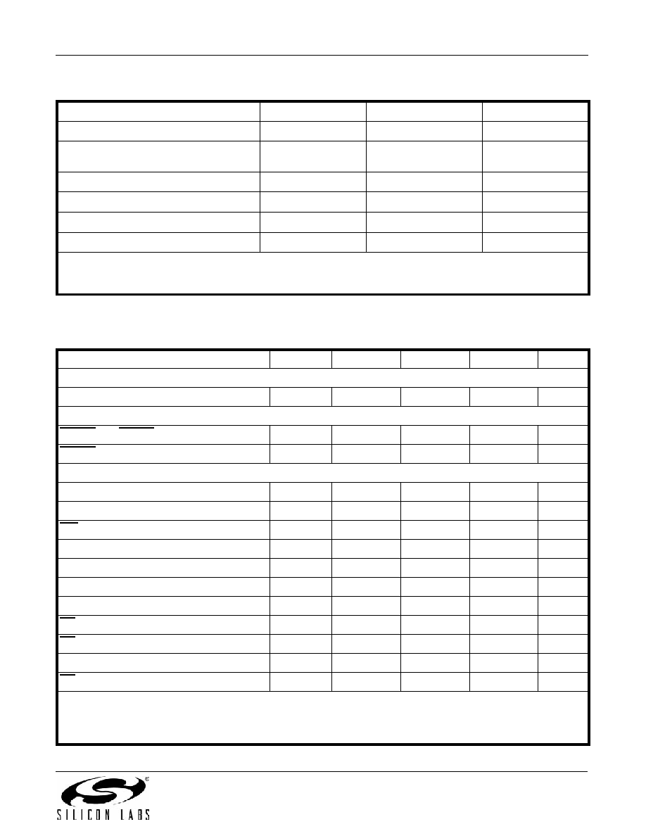
Table 5. Absolute Maximum Ratings
Parameter
Symbol
Value
Unit
DC Supply Voltage
VD
4.1
V
Input Current, Si2457/34/15/04 Digital
Input Pins
IIN
±10
mA
Digital Input Voltage
VIND
–0.3 to (VD + 0.3)
V
CLKIN/XTALI Input Voltage
VXIND
–0.3 to (VD + 0.3)
V
Operating Temperature Range
TA
–10 to 100
°C
Storage Temperature Range
TSTG
–40 to 150
°C
Note: Permanent device damage may occur if the above absolute maximum ratings are exceeded. Functional operation
should be restricted to the conditions as specified in the operational sections of this data sheet. Exposure to absolute
maximum rating conditions for extended periods may affect device reliability.
Table 6. Switching Characteristics1
(VD = 3.0 to 3.6 V, TA = 0 to 70 °C for F-grade, TA = –40 to 85 °C for G-grade)
Parameter
Symbol
Min
Typ
Max
Unit
UART Timing Parameters
Baud Rate Accuracy
tBD
–1
—
1
%
Reset Timing Parameters
RESET
to RESET
tRS
5.02
——
ms
RESET
to 1st AT Command
tAT
300
—
ms
Parallel Timing Parameters
Address Setup
tAS
15
—
ns
Address Hold
tAH
0—
—
ns
WR Low Pulse Width
tWL
50
—
ns
Write Data Setup Time
tWDSU
20
—
ns
Write Cycle Time
tWC
120
—
ns
Chip Select Setup
tCSS
10
—
ns
Chip Select Hold
tCSH
0—
—
ns
RD Low Pulse Width
tRL
50
—
ns
RD Low to Data Driven Time
tRLDD
—
20
ns
Data Hold
tDH
10
—
ns
RD High to Hi-Z Time
tDZ
—
30
ns
Notes:
1. All timing is referenced to the 50% level of the waveform. Input test levels are VIH =VD – 0.4 V, VIL =0.4 V.
2. With 32.768 kHz clocking, allow 500 ms for the reset low-to-high minimum pulse on power-up and wake-from-power-
down conditions.
相關(guān)PDF資料 |
PDF描述 |
|---|---|
| VE-J6Y-IX-B1 | CONVERTER MOD DC/DC 3.3V 49.5W |
| VI-2N2-IX-F2 | CONVERTER MOD DC/DC 15V 75W |
| VI-2N2-IX-F1 | CONVERTER MOD DC/DC 15V 75W |
| VI-2N1-IX-F4 | CONVERTER MOD DC/DC 12V 75W |
| VE-J6Y-IW-B1 | CONVERTER MOD DC/DC 3.3V 66W |
相關(guān)代理商/技術(shù)參數(shù) |
參數(shù)描述 |
|---|---|
| SI2415-D-GTR | 制造商:Silicon Laboratories Inc 功能描述:14.4 KBPS ISOMODEM SYSTEM-SIDE 制造商:Silicon Laboratories Inc 功能描述:14.4 KBPS ISOMODEM SYSTEM-SIDE - LEAD-FREE - Tape and Reel 制造商:Silicon Laboratories Inc 功能描述:IC ISOMODEM GLOBAL DAA 24TSSOP 制造商:Silicon Laboratories Inc 功能描述:14.4 kbps ISOmodem System-Side PBF |
| Si2415FS08-EVB | 功能描述:網(wǎng)絡(luò)開(kāi)發(fā)工具 16-pin Si2415+Si3008 ISOmodem Eval Board RoHS:否 制造商:Rabbit Semiconductor 產(chǎn)品:Development Kits 類(lèi)型:Ethernet to Wi-Fi Bridges 工具用于評(píng)估:RCM6600W 數(shù)據(jù)速率:20 Mbps, 40 Mbps 接口類(lèi)型:802.11 b/g, Ethernet 工作電源電壓:3.3 V |
| Si2415FS18-EVB | 功能描述:網(wǎng)絡(luò)開(kāi)發(fā)工具 16-pin Si2415+Si3018 ISOmodem Eval Board RoHS:否 制造商:Rabbit Semiconductor 產(chǎn)品:Development Kits 類(lèi)型:Ethernet to Wi-Fi Bridges 工具用于評(píng)估:RCM6600W 數(shù)據(jù)速率:20 Mbps, 40 Mbps 接口類(lèi)型:802.11 b/g, Ethernet 工作電源電壓:3.3 V |
| SI2415-FT | 功能描述:電信線路管理 IC RoHS:否 制造商:STMicroelectronics 產(chǎn)品:PHY 接口類(lèi)型:UART 電源電壓-最大:18 V 電源電壓-最小:8 V 電源電流:30 mA 最大工作溫度:+ 85 C 最小工作溫度:- 40 C 安裝風(fēng)格:SMD/SMT 封裝 / 箱體:VFQFPN-48 封裝:Tray |
| Si2415FT08-EVB | 功能描述:網(wǎng)絡(luò)開(kāi)發(fā)工具 24-pin Si2415+Si3008 ISOmodem Eval Board RoHS:否 制造商:Rabbit Semiconductor 產(chǎn)品:Development Kits 類(lèi)型:Ethernet to Wi-Fi Bridges 工具用于評(píng)估:RCM6600W 數(shù)據(jù)速率:20 Mbps, 40 Mbps 接口類(lèi)型:802.11 b/g, Ethernet 工作電源電壓:3.3 V |
發(fā)布緊急采購(gòu),3分鐘左右您將得到回復(fù)。