- 您現(xiàn)在的位置:買賣IC網(wǎng) > PDF目錄373432 > SN54ABT162600 (Texas Instruments, Inc.) 18-Bit Universal Bus Transceivers With 3-State Outputs(18位通用總線收發(fā)器(三態(tài)輸出)) PDF資料下載
參數(shù)資料
| 型號: | SN54ABT162600 |
| 廠商: | Texas Instruments, Inc. |
| 英文描述: | 18-Bit Universal Bus Transceivers With 3-State Outputs(18位通用總線收發(fā)器(三態(tài)輸出)) |
| 中文描述: | 18位通用總線收發(fā)器與三態(tài)輸出(18位通用總線收發(fā)器(三態(tài)輸出)) |
| 文件頁數(shù): | 1/8頁 |
| 文件大?。?/td> | 175K |
| 代理商: | SN54ABT162600 |
SN54ABT162600, SN74ABT162600
18-BIT UNIVERSAL BUS TRANSCEIVERS
WITH 3-STATE OUTPUTS
SCBS246 – JUNE 1992 – REVISED OCTOBER 1992
POST OFFICE BOX 655303
DALLAS, TEXAS 75265
Copyright
1992, Texas Instruments Incorporated
6–1
B-Port Outputs Have Equivalent 25-
Series Resistors, So No External Resistors
Are Required
Members of the Texas Instruments
Widebus
Family
State-of-the-Art EPIC-
ΙΙ
B
BiCMOS Design
Significantly Reduces Power Dissipation
UBT
(Universal Bus Transceiver)
Combines D-Type Latches and D-Type
Flip-Flops for Operation in Transparent,
Latched, Clocked, or Clock-Enabled Mode
ESD Protection Exceeds 2000 V Per
MIL-STD-883C, Method 3015; Exceeds
200 V Using Machine Model
(C = 200 pF, R = 0)
Latch-Up Performance Exceeds 500 mA
Per JEDEC Standard JESD-17
Typical V
OLP
(Output Ground Bounce)
< 0.8 V at V
CC
= 5 V, T
A
= 25
°
C
Flow-Through Architecture Optimizes
PCB Layout
Packaged in Plastic 300-mil Shrink
Small-Outline Packages and 380-mil
Fine-Pitch Ceramic Flat Packages Using
25-mil Center-to-Center Spacings
description
These 18-bit universal bus transceivers combine
D-type latches and D-type flip-flops to allow data
flow in transparent, latched, and clocked modes.
Data flow in each direction is controlled by output-enable (OEAB and OEBA), latch-enable (LEAB and LEBA),
and clock (CLKAB and CLKBA) inputs. The clock can be controlled by the clock-enable (CLKENAB and
CLKENBA) inputs. For A-to-B data flow, the device operates in the transparent mode when LEAB is high. When
LEAB is low, the A data is latched if CLKAB is held at a high or low logic level. If LEAB is low, the A-bus data
is stored in the latch/flip-flop on the high-to-low transition of CLKAB. Output-enable OEAB is active-low. When
OEAB is low, the outputs are active. When OEAB is high, the outputs are in the high-impedance state. Data flow
for B to A is similar to that of A to B but uses OEBA, LEBA, CLKBA, and CLKENBA.
The B-port outputs, which are designed to source or sink up to 12 mA, include 25-
series resistors to reduce
overshoot and undershoot.
To ensure the high-impedance state during power up or power down, OE should be tied to V
CC
through a pullup
resistor; the minimum value of the resistor is determined by the current-sinking capability of the driver.
The SN74ABT162600 is available in TI’s shrink small-outline package (DL), which provides twice the I/O pin
count and functionality of standard small-outline packages in the same printed-circuit-board area.
The SN54ABT162600 is characterized over the full military temperature range of –55
°
C to 125
°
C. The
SN74ABT162600 is characterized for operation from –40
°
C to 85
°
C.
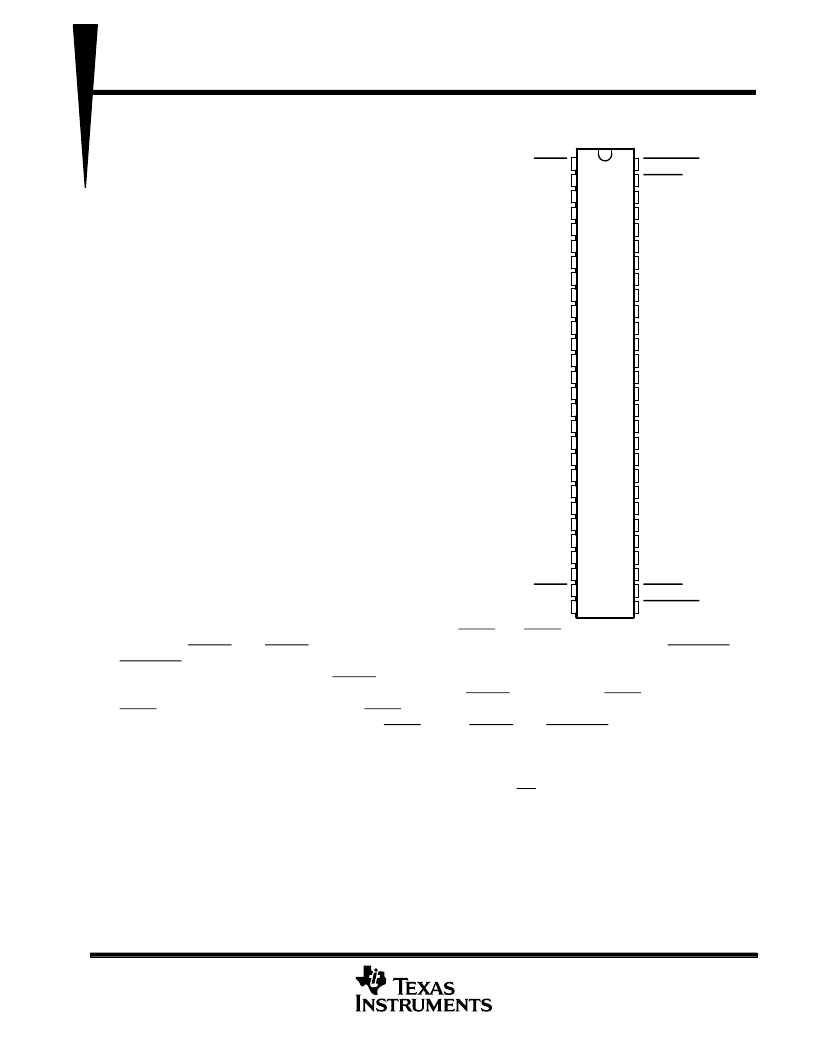
ABT162600–1
SN54ABT162600 . . . WD PACKAGE
SN74ABT162600 . . . DL PACKAGE
(TOP VIEW)
1
2
3
4
5
6
7
8
9
10
11
12
13
14
15
16
17
18
19
20
21
22
23
24
25
26
27
28
56
55
54
53
52
51
50
49
48
47
46
45
44
43
42
41
40
39
38
37
36
35
34
33
32
31
30
29
OEAB
LEAB
A1
GND
A2
A3
V
CC
A4
A5
A6
GND
A7
A8
A9
A10
A11
A12
GND
A13
A14
A15
V
CC
A16
A17
GND
A18
OEBA
LEBA
CLKENAB
CLKAB
B1
GND
B2
B3
V
CC
B4
B5
B6
GND
B7
B8
B9
B10
B11
B12
GND
B13
B14
B15
V
CC
B16
B17
GND
B18
CLKBA
CLKENBA
Widebus, EPIC-
ΙΙ
B, and UBT are trademarks of Texas Instruments Incorporated.
PRODUCT PREVIEW information concerns products in the formative or
design phase of development. Characteristic data and other
specifications are design goals. Texas Instruments reserves the right to
change or discontinue these products without notice.
P
相關(guān)PDF資料 |
PDF描述 |
|---|---|
| SN74ABT162600 | 18-Bit Universal Bus Transceivers With 3-State Outputs(18位通用總線收發(fā)器(三態(tài)輸出)) |
| SN54ABT16265 | 12-Bit to 24-Bit Multiplexed Transceivers With 3-State Outputs(12-24多路收發(fā)器(三態(tài)輸出)) |
| SN74ABT16265 | 12-Bit to 24-Bit Multiplexed Transceivers With 3-State Outputs(12-24多路收發(fā)器(三態(tài)輸出)) |
| SN54ABT162823 | 18-Bit Bus-Interface Flip-Flops 3-State Outputs(18位總線接口觸發(fā)器(三態(tài)輸出)) |
| SN54ABT16374AWD | 16-BIT EDGE-TRIGGERED D-TYPE FLIP-FLOPS WITH 3-STATE OUTPUTS |
相關(guān)代理商/技術(shù)參數(shù) |
參數(shù)描述 |
|---|---|
| SN54ABT162601 | 制造商:TI 制造商全稱:Texas Instruments 功能描述:18-BIT UNIVERSAL BUS TRANSCEIVERS WITH 3-STATE OUTPUTS |
| SN54ABT162601WD | 制造商:TI 制造商全稱:Texas Instruments 功能描述:18-BIT UNIVERSAL BUS TRANSCEIVERS WITH 3-STATE OUTPUTS |
| SN54ABT16260WD | 制造商:TI 制造商全稱:Texas Instruments 功能描述:12-BIT TO 24-BIT MULTIPLEXED D-TYPE LATCHES WITH 3-STATE OUTPUTS |
| SN54ABT162823 | 制造商:TI 制造商全稱:Texas Instruments 功能描述:18-BIT BUS-INTERFACE FLIP-FLOPS WITH 3-STATE OUTPUTS |
| SN54ABT162823A | 制造商:TI 制造商全稱:Texas Instruments 功能描述:18-BIT BUS-INTERFACE FLIP-FLOPS WITH 3-STATE OUTPUTS |
發(fā)布緊急采購,3分鐘左右您將得到回復(fù)。