- 您現(xiàn)在的位置:買賣IC網(wǎng) > PDF目錄373432 > SN54ABT16843 (Texas Instruments, Inc.) 18-Bit Bus-Interface D-Type Latches With 3-State Outputs(18位總線接口D鎖存器(三態(tài)輸出)) PDF資料下載
參數(shù)資料
| 型號(hào): | SN54ABT16843 |
| 廠商: | Texas Instruments, Inc. |
| 英文描述: | 18-Bit Bus-Interface D-Type Latches With 3-State Outputs(18位總線接口D鎖存器(三態(tài)輸出)) |
| 中文描述: | 18位總線接口D類鎖存器與三態(tài)輸出(18位總線接口?鎖存器(三態(tài)輸出)) |
| 文件頁數(shù): | 1/8頁 |
| 文件大?。?/td> | 182K |
| 代理商: | SN54ABT16843 |
SN54ABT16843, SN74ABT16843
18-BIT BUS-INTERFACE D-TYPE LATCHES
WITH 3-STATE OUTPUTS
SCBS223E – OCTOBER 1992 – REVISED MAY 1997
1
POST OFFICE BOX 655303
DALLAS, TEXAS 75265
Members of the Texas Instruments
Widebus
Family
State-of-the-Art EPIC-
ΙΙ
B
BiCMOS Design
Significantly Reduces Power Dissipation
Distributed V
CC
and GND Pin Configuration
Minimizes High-Speed Switching Noise
Flow-Through Architecture Optimizes PCB
Layout
High-Impedance State During Power Up
and Power Down
High-Drive Outputs (–32-mA I
OH
, 64-mA I
OL
)
Package Options Include Plastic Thin
Shrink Small-Outline (DGG), 300-mil Shrink
Small-Outline (DL) Packages and 380-mil
Fine-Pitch Ceramic Flat (WD) Package
Using 25-mil Center-to-Center Spacings
description
The ’ABT16843 18-bit bus-interface D-type
latches are designed specifically for driving highly
capacitive or relatively low-impedance loads.
They are particularly suitable for implementing
buffer registers, I/O ports, bidirectional bus
drivers, and working registers.
The ’ABT16843 can be used as two 9-bit latches
or one 18-bit latch. The 18 latches are transparent
D-type latches. The device provides true data at
its outputs.
A buffered output-enable (OE) input can be used
to place the nine outputs in either a normal logic
state
(high
or
low
high-impedance state. The outputs are in the
high-impedance state during power up and power
down. The outputs remain in the high-impedance
state while the device is powered down. In the
high-impedance state, the outputs neither load
nor drive the bus lines significantly. The
high-impedance state and increased drive
provide the capability to drive bus lines without
need for interface or pullup components.
logic
levels)
or
a
1
2
3
4
5
6
7
8
9
10
11
12
13
14
15
16
17
18
19
20
21
22
23
24
25
26
27
28
56
55
54
53
52
51
50
49
48
47
46
45
44
43
42
41
40
39
38
37
36
35
34
33
32
31
30
29
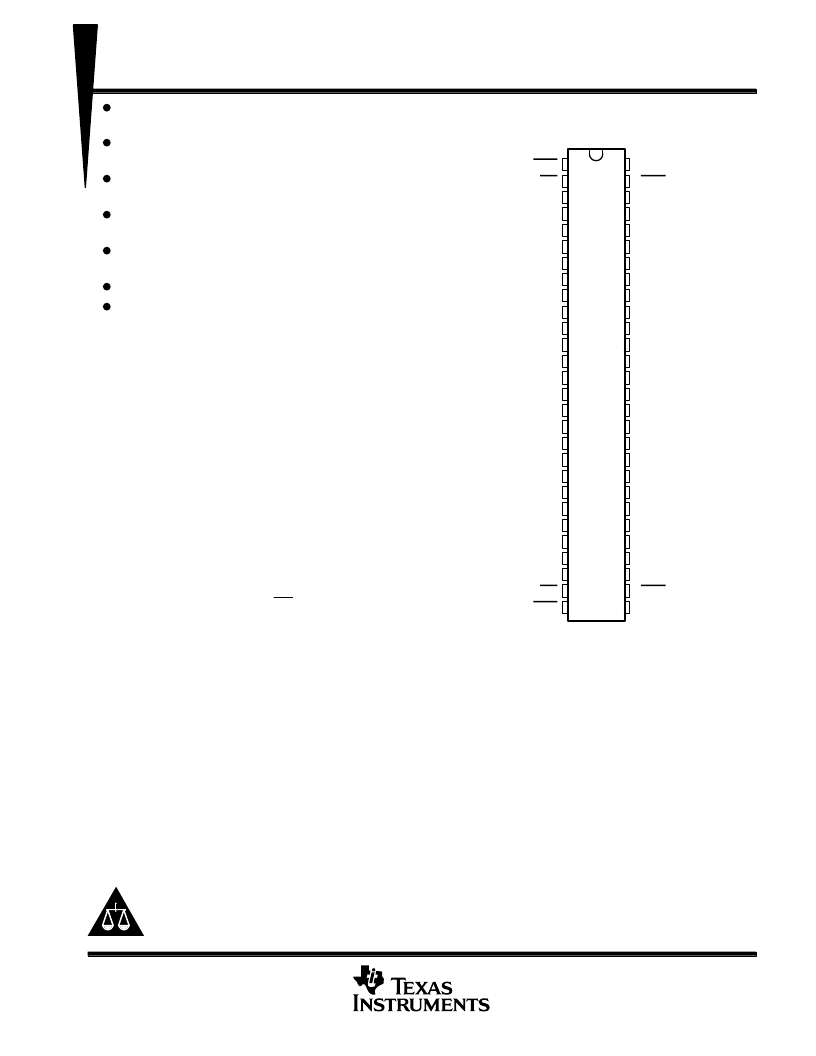
1CLR
1OE
1Q1
GND
1Q2
1Q3
V
CC
1Q4
1Q5
1Q6
GND
1Q7
1Q8
1Q9
2Q1
2Q2
2Q3
GND
2Q4
2Q5
2Q6
V
CC
2Q7
2Q8
GND
2Q9
2OE
2CLR
1LE
1PRE
1D1
GND
1D2
1D3
V
CC
1D4
1D5
1D6
GND
1D7
1D8
1D9
2D1
2D2
2D3
GND
2D4
2D5
2D6
V
CC
2D7
2D8
GND
2D9
2PRE
2LE
SN54ABT16843 . . . WD PACKAGE
SN74ABT16843 . . . DGG OR DL PACKAGE
(TOP VIEW)
Copyright
1997, Texas Instruments Incorporated
UNLESS OTHERWISE NOTED this document contains PRODUCTION
DATA information current as of publication date. Products conform to
specifications per the terms of Texas Instruments standard warranty.
Production processing does not necessarily include testing of all
parameters.
Widebus and EPIC-
ΙΙ
B are trademarks of Texas Instruments Incorporated.
Please be aware that an important notice concerning availability, standard warranty, and use in critical applications of
Texas Instruments semiconductor products and disclaimers thereto appears at the end of this data sheet.
相關(guān)PDF資料 |
PDF描述 |
|---|---|
| SN54ABT16853 | Dual 8-Bit to 9-Bit Parity Bus Transceivers(雙8-9奇偶總線收發(fā)器) |
| SN54ABT16863WD | 18-BIT BUS TRANSCEIVERS WITH 3-STATE OUTPUTS |
| SN54ABT16952WD | 16-BIT REGISTERED TRANSCEIVERS WITH 3-STATE OUTPUTS |
| SN74ABT16952DGG | 16-BIT REGISTERED TRANSCEIVERS WITH 3-STATE OUTPUTS |
| SN54ABT16952 | 16-Bit Registered Transceivers With 3-State Outputs(16位記錄收發(fā)器(三態(tài)輸出)) |
相關(guān)代理商/技術(shù)參數(shù) |
參數(shù)描述 |
|---|---|
| SN54ABT16843_08 | 制造商:TI 制造商全稱:Texas Instruments 功能描述:18-BIT BUS-INTERFACE D-TYPE LATCHES WITH 3-STATE OUTPUTS |
| SN54ABT16843WD | 制造商:TI 制造商全稱:Texas Instruments 功能描述:18-BIT BUS-INTERFACE D-TYPE LATCHES WITH 3-STATE OUTPUTS |
| SN54ABT16853 | 制造商:TI 制造商全稱:Texas Instruments 功能描述:DUAL 8-BIT TO 9-BIT PARITY BUS TRANSCEIVERS |
| SN54ABT16853_06 | 制造商:TI 制造商全稱:Texas Instruments 功能描述:DUAL 8-BIT TO 9-BIT PARITY BUS TRANSCEIVERS |
| SN54ABT16853_07 | 制造商:TI 制造商全稱:Texas Instruments 功能描述:DUAL 8-BIT TO 9-BIT PARITY BUS TRANSCEIVERS |
發(fā)布緊急采購,3分鐘左右您將得到回復(fù)。