- 您現(xiàn)在的位置:買賣IC網(wǎng) > PDF目錄373462 > SN54LVTZ245 (Texas Instruments, Inc.) 3.3V ABT Octal Buffers/Drivers With 3-State Outputs(3.3 ABT 八緩沖器/驅(qū)動(dòng)器(三態(tài)輸出)) PDF資料下載
參數(shù)資料
| 型號(hào): | SN54LVTZ245 |
| 廠商: | Texas Instruments, Inc. |
| 英文描述: | 3.3V ABT Octal Buffers/Drivers With 3-State Outputs(3.3 ABT 八緩沖器/驅(qū)動(dòng)器(三態(tài)輸出)) |
| 中文描述: | 3.3生根粉八路緩沖器/驅(qū)動(dòng)器與3態(tài)輸出(3.3 ABT生根粉八緩沖器/驅(qū)動(dòng)器(三態(tài)輸出)) |
| 文件頁(yè)數(shù): | 2/7頁(yè) |
| 文件大小: | 149K |
| 代理商: | SN54LVTZ245 |
SN54LVTZ245, SN74LVTZ245
3.3-V ABT OCTAL BUS TRANSCEIVERS
WITH 3-STATE OUTPUTS
SCBS303C – DECEMBER 1993 – REVISED JANUARY 1996
2
POST OFFICE BOX 655303
DALLAS, TEXAS 75265
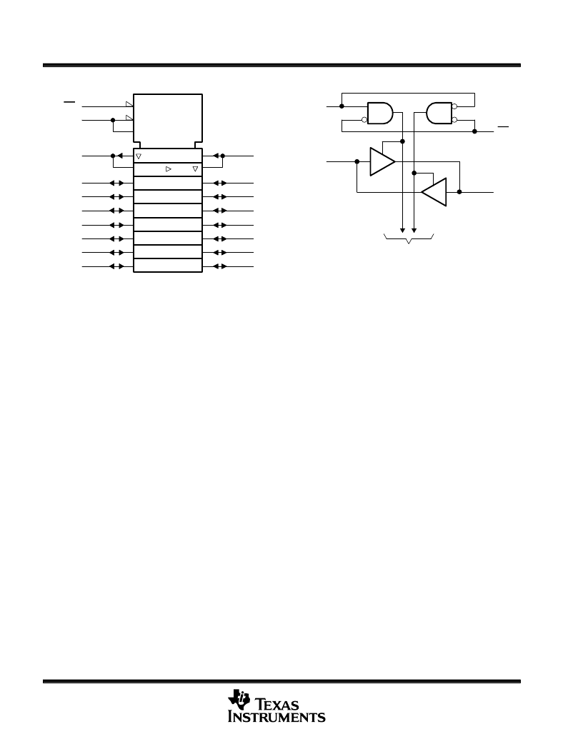
logic symbol
logic diagram (positive logic)
B2
17
B3
16
B4
15
A5
6
A6
7
A7
8
A8
9
A2
3
A3
4
A4
5
OE
A1
2
G3
19
3EN2[AB]
B5
14
B6
13
B7
12
B8
11
B1
18
3EN1[BA]
1
DIR
DIR
OE
A1
B1
1
2
18
19
To Seven Other Channels
1
2
This symbol is in accordance with ANSI/IEEE Std 91-1984
and IEC Publication 617-12.
Pin numbers shown are for the DB, DW, PW, and J packages.
absolute maximum ratings over operating free-air temperature range (unless otherwise noted)
Supply voltage range, V
CC
Input voltage range, V
I
(see Note 1)
Voltage range applied to any output in the high state or power-off state, V
O
(see Note 1)
Current into any output in the low state, I
O
: SN54LVTZ245
SN74LVTZ245
Current into any output in the high state, I
O
(see Note 2): SN54LVTZ245
–0.5 V to 4.6 V
–0.5 V to 7 V
–0.5 V to 7 V
. . . .
. . . . . . . . . . . . . . . . . . . . . . . . . . . . . . . . . . . . . . . . . . . . . . . . . . . . . . . .
. . . . . . . . . . . . . . . . . . . . . . . . . . . . . . . . . . . . . . . . . . . . . . . . . .
96 mA
128 mA
48 mA
64 mA
–50 mA
–50 mA
0.6 W
1.6 W
0.7 W
. . . . . . . . . . . . . . . . . . . . . . . . . . . . . . . . . . . .
. . . . . . . . . . . . . . . . . . . . . . . . . . . . . . . . . . .
. . . . . . . . . . . . . . . . . . . . . . . .
SN74LVTZ245
. . . . . . . . . . . . . . . . . . . . . . . .
Input clamp current, I
IK
(V
I
< 0)
Output clamp current, I
OK
(V
O
< 0)
Maximum power dissipation at T
A
= 55
°
C (in still air) (see Note 3):DB package
. . . . . . . . . . . . . . . . . . . . . . . . . . . . . . . . . . . . . . . . . . . . . . . . . . . . . . . . . .
. . . . . . . . . . . . . . . . . . . . . . . . . . . . . . . . . . . . . . . . . . . . . . . . . . . . . . .
. . . . . . . . . . . . . . . . . . . .
. . . . . . . . . . . . . . . . . . .
. . . . . . . . . . . . . . . . . . .
DW package
PW package
Storage temperature range, T
stg
Stresses beyond those listed under “absolute maximum ratings” may cause permanent damage to the device. These are stress ratings only, and
functional operation of the device at these or any other conditions beyond those indicated under “recommended operating conditions” is not
implied. Exposure to absolute-maximum-rated conditions for extended periods may affect device reliability.
NOTES:
1. The input and output negative-voltage ratings may be exceeded if the input and output clamp-current ratings are observed.
2. This current flows only when the output is in the high state and VO > VCC.
3. The maximum package power dissipation is calculated using a junction temperature of 150
°
C and a board trace length of 750 mils.
For more information, refer to the Package Thermal Considerationsapplication note in the 1994 ABT Advanced BiCMOS Technology
Data Book literature number SCBD002B.
–65
°
C to 150
°
C
. . . . . . . . . . . . . . . . . . . . . . . . . . . . . . . . . . . . . . . . . . . . . . . . . .
相關(guān)PDF資料 |
PDF描述 |
|---|---|
| SN54S11W | Host-controlled Synchronous, Switch-Mode Li-Ion Charger w/2A FET in QFN-20, 1 to 3 cells 20-QFN -40 to 85 |
| SN54S11FK | TRIPLE 3-INPUT POSITIVE-AND GATES |
| SN54LS11FK | TRIPLE 3-INPUT POSITIVE-AND GATES |
| SN54LS11W | TRIPLE 3-INPUT POSITIVE-AND GATES |
| SN54LS11J | TRIPLE 3-INPUT AND GATE |
相關(guān)代理商/技術(shù)參數(shù) |
參數(shù)描述 |
|---|---|
| SN54S00J | 制造商:Texas Instruments 功能描述:NAND Gate 4-Element 2-IN Bipolar 14-Pin CDIP Tube 制造商:Rochester Electronics LLC 功能描述:- Bulk |
| SN54S00W | 制造商:Rochester Electronics LLC 功能描述:- Bulk |
| SN54S02J | 制造商:Texas Instruments 功能描述: |
| SN54S03J | 制造商:Rochester Electronics LLC 功能描述:- Bulk 制造商:Texas Instruments 功能描述:2-INPUT NAND GATE (OC) - Rail/Tube |
| SN54S04J | 制造商:Texas Instruments 功能描述:Inverter 6-Element Bipolar 14-Pin CDIP Tube 制造商:Rochester Electronics LLC 功能描述:- Bulk 制造商:Texas Instruments 功能描述:INVERTER 6-ELEM BIPOLAR 14CDIP - Rail/Tube 制造商:Texas Instruments 功能描述:HEX INVERTER *NIC* |
發(fā)布緊急采購(gòu),3分鐘左右您將得到回復(fù)。