- 您現(xiàn)在的位置:買賣IC網(wǎng) > PDF目錄299917 > SN75ALS180NE4 (TEXAS INSTRUMENTS INC) LINE TRANSCEIVER, PDIP14 PDF資料下載
參數(shù)資料
| 型號: | SN75ALS180NE4 |
| 廠商: | TEXAS INSTRUMENTS INC |
| 元件分類: | Buffer和線驅(qū)動 |
| 英文描述: | LINE TRANSCEIVER, PDIP14 |
| 封裝: | ROHS COMPLIANT, PLASTIC, DIP-14 |
| 文件頁數(shù): | 16/21頁 |
| 文件大小: | 555K |
| 代理商: | SN75ALS180NE4 |
SN65ALS180, SN75ALS180
DIFFERENTIAL DRIVER AND RECEIVER PAIRS
SLLS052G – AUGUST 1987 – REVISED APRIL 2003
4
POST OFFICE BOX 655303
DALLAS, TEXAS 75265
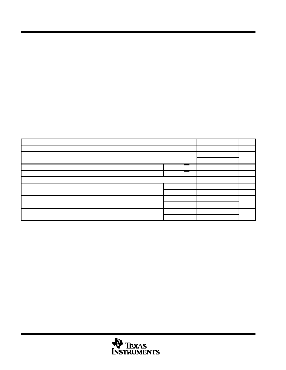
absolute maximum ratings over operating free-air temperature range (unless otherwise noted)
Supply voltage, VCC (see Note 1)
7 V
. . . . . . . . . . . . . . . . . . . . . . . . . . . . . . . . . . . . . . . . . . . . . . . . . . . . . . . . . . . . .
Voltage range at any bus terminal
–10 V to 15 V
. . . . . . . . . . . . . . . . . . . . . . . . . . . . . . . . . . . . . . . . . . . . . . . . . . . .
Enable input voltage, VI
5.5 V
. . . . . . . . . . . . . . . . . . . . . . . . . . . . . . . . . . . . . . . . . . . . . . . . . . . . . . . . . . . . . . . . . . . .
Package thermal impedance,
θJA (see Notes 2 and 3): D package
86
°C/W
. . . . . . . . . . . . . . . . . . . . . . . . . . . .
N package
80
°C/W
. . . . . . . . . . . . . . . . . . . . . . . . . . . .
Operating virtual junction temperature, TJ
150
°C
. . . . . . . . . . . . . . . . . . . . . . . . . . . . . . . . . . . . . . . . . . . . . . . . . . .
Lead temperature 1,6 mm (1/16 inch) from case for 10 seconds
260
°C
. . . . . . . . . . . . . . . . . . . . . . . . . . . . . . .
Storage temperature range, Tst
–65
°C to 150°C
. . . . . . . . . . . . . . . . . . . . . . . . . . . . . . . . . . . . . . . . . . . . . . . . . . . .
Stresses beyond those listed under “absolute maximum ratings” may cause permanent damage to the device. These are stress ratings only, and
functional operation of the device at these or any other conditions beyond those indicated under “recommended operating conditions” is not
implied. Exposure to absolute-maximum-rated conditions for extended periods may affect device reliability.
NOTES:
1. All voltage values, except differential I/O bus voltage, are with respect to network ground terminal.
2. Maximum power dissipation is a function of TJ(max), θJA, and TA. The maximum allowable power dissipation at any allowable
ambient temperature is PD = (TJ(max) – TA)/θJA. Operating at the absolute maximum TJ of 150°C can affect reliability.
3. The package thermal impedance is calculated in accordance with JESD 51-7.
recommended operating conditions
MIN
NOM
MAX
UNIT
VCC
Supply voltage
4.75
5
5.25
V
VI or VIC
Voltage at any bus terminal (separately or common mode)
12
V
VI or VIC
Voltage at any bus terminal (separately or common mode)
–7
V
VIH
High-level input voltage
D, DE, and RE
2
V
VIL
Low-level input voltage
D, DE, and RE
0.8
V
VID
Differential input voltage (see Note 4)
±12
V
IOH
High level output current
Driver
–60
mA
IOH
High-level output current
Receiver
–400
A
IOL
Low level output current
Driver
60
mA
IOL
Low-level output current
Receiver
8
mA
TA
Operating free air temperature
SN65ALS180
–40
85
°C
TA
Operating free-air temperature
SN75ALS180
0
70
°C
NOTE 4: Differential-input/output bus voltage is measured at the noninverting terminal, A/Y, with respect to the inverting terminal, B/Z.
相關PDF資料 |
PDF描述 |
|---|---|
| SN75C1154NE4 | QUAD LINE TRANSCEIVER, PDIP20 |
| SN75C1154NSRE4 | QUAD LINE TRANSCEIVER, PDSO20 |
| SN75C3223EDBG4 | DUAL LINE TRANSCEIVER, PDSO20 |
| SN75C3223EDBRG4 | DUAL LINE TRANSCEIVER, PDSO20 |
| SN75C3223EDBR | DUAL LINE TRANSCEIVER, PDSO20 |
相關代理商/技術參數(shù) |
參數(shù)描述 |
|---|---|
| SN75ALS181 | 制造商:TI 制造商全稱:Texas Instruments 功能描述:DIFFERENTIAL DRIVER AND RECEIVER PAIR |
| SN75ALS181_08 | 制造商:TI 制造商全稱:Texas Instruments 功能描述:DIFFERENTIAL DRIVER AND RECEIVER PAIR |
| SN75ALS181_10 | 制造商:TI 制造商全稱:Texas Instruments 功能描述:DIFFERENTIAL DRIVER AND RECEIVER PAIR |
| SN75ALS181N | 功能描述:RS-422/RS-485 接口 IC Diff Pairs RoHS:否 制造商:Maxim Integrated 數(shù)據(jù)速率:1136 Kbps 工作電源電壓:3 V to 5.5 V 電源電流:5.9 mA 工作溫度范圍:- 40 C to + 85 C 安裝風格:SMD/SMT 封裝 / 箱體:SOIC-28 封裝:Tube |
| SN75ALS181N | 制造商:Texas Instruments 功能描述:LEADED PROCESS COMPATIBLE ((NW)) 制造商:Texas Instruments 功能描述:IC, RS422/RS485 TRANSCEIVER, 5.25V DIP14 |
發(fā)布緊急采購,3分鐘左右您將得到回復。