- 您現(xiàn)在的位置:買賣IC網(wǎng) > PDF目錄372179 > SP3249 5V High-Speed RS-232 Transceivers with 0.1uF Capacitors PDF資料下載
參數(shù)資料
| 型號: | SP3249 |
| 元件分類: | RS-232 |
| 英文描述: | 5V High-Speed RS-232 Transceivers with 0.1uF Capacitors |
| 中文描述: | 5V的高速RS - 232收發(fā)器與0.1uF電容 |
| 文件頁數(shù): | 2/14頁 |
| 文件大小: | 128K |
| 代理商: | SP3249 |

Rev.4/08/02
SP3249E Intelligent +3.0V to +5.5V RS-232 Transceivers
2
Copyright 2002 Sipex Corporation
ABSOLUTE MAXIMUM RATINGS
These are stress ratings only and functional operation
of the device at these ratings or any other above those
indicated in the operation sections of the specifications
below is not implied. Exposure to absolute maximum
rating conditions for extended periods of time may
affect reliability and cause permanent damage to the
device.
V
.......................................................-0.3V to +6.0V
V+ (NOTE 1).......................................-0.3V to +7.0V
V- (NOTE 1)........................................+0.3V to -7.0V
V+ + |V-| (NOTE 1)...........................................+13V
I
CC
(DC V
CC
or GND current).........................+100mA
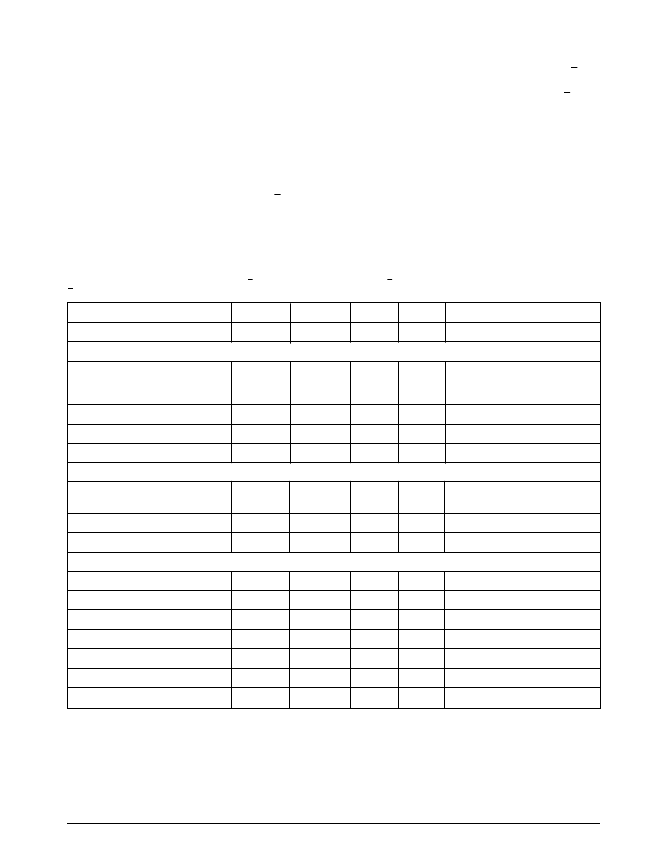
SPECIFICATIONS
V
= +3.0 to +5.5, C1 -C4 = 0.1
μ
F (tested at 3.3V + 5%), C1-C4 = 0.22
μ
F (tested at 3.3V + 10%), C1 = 0.047
μ
F, and C2-C4 = 0.33
μ
F (tested at 5.0V
+ 10%), T
A
= T
MIN
to T
MAX
, unless otherwise noted. Typical values are at T
A
= +25
°
C.)
Note 1: V+ and V- can have maximum magnitudes of 7V, but their absolute difference cannot exceed 13V.
Input Voltages
TxIN ...................................................-0.3V to +6.0V
RxIN...................................................................+25V
Output Voltages
TxOUT.............................................................+13.2V
RxOUT,......................................-0.3V to (V
CC
+ 0.3V)
Short-Circuit Duration
TxOUT.....................................................Continuous
Storage Temperature......................-65
°
C to +150
°
C
PARAMETER
MIN.
TYP.
MAX.
UNITS
CONDITIONS
Supply Current
0.3
1.0
mA
V
CC
, no load
LOGIC INPUTS AND RECEIVER OUTPUTS
Input Logic Threshold
LOW
HIGH
0.8
V
V
V
CC
= +3.3V or +5.0V, TxIN
V
CC
= +3.3V or +5.0V, TxIN
2.4
Input Leakage Current
±
0.01
±
1.0
μ
A
TxIN, T
A
= 25
°
C
Output Voltage LOW
0.4
V
I
OUT
= 1.6mA
Output Voltage HIGH
V
CC
- 0.6
V
CC
- 0.1
V
I
OUT
= -1.0mA
DRIVER OUTPUTS
Output Voltage Swing
±
5.0
±
5.4
V
All driver outputs loaded with
3K
to GND
Output Resistance
300
V
CC
= V+ = V- = 0V, V
OUT
=
±
2V
Output Short-Circuit Current
±
35
±
60
mA
V
OUT
= GND
RECEIVER INPUTS
Input Voltage Range
-25
25
V
Input Threshold LOW
0.6
1.2
V
V
CC
= 3.3V
Input Threshold LOW
0.8
1.5
V
V
CC
= 5.0V
Input Threshold HIGH
1.5
2.4
V
V
CC
= 3.3V
Input Threshold HIGH
1.8
2.4
V
V
CC
= 5.0V
Input Hysteresis
0.5
V
Input Resistance
3
5
7
k
相關(guān)PDF資料 |
PDF描述 |
|---|---|
| SP3239E | 5V High-Speed RS-232 Transceivers with 0.1uF Capacitors |
| SP3281EBCA | 5V High-Speed RS-232 Transceivers with 0.1uF Capacitors |
| SP3281EB | 5V High-Speed RS-232 Transceivers with 0.1uF Capacitors |
| SP3281EBCY | 5V High-Speed RS-232 Transceivers with 0.1uF Capacitors |
| SP3281EBEA | 5V High-Speed RS-232 Transceivers with 0.1uF Capacitors |
相關(guān)代理商/技術(shù)參數(shù) |
參數(shù)描述 |
|---|---|
| SP3249E | 制造商:SIPEX 制造商全稱:Sipex Corporation 功能描述:Intelligent +3.0V to +5.5V RS-232 Transceivers |
| SP3249ECA | 制造商:SIPEX 制造商全稱:Sipex Corporation 功能描述:Intelligent +3.0V to +5.5V RS-232 Transceivers |
| SP3249ECA-L | 制造商:Rochester Electronics LLC 功能描述: 制造商:Exar Corporation 功能描述: |
| SP3249ECA-L/TR | 制造商:Rochester Electronics LLC 功能描述: 制造商:Exar Corporation 功能描述: |
| SP3249ECY | 制造商:Rochester Electronics LLC 功能描述: 制造商:Exar Corporation 功能描述: |
發(fā)布緊急采購,3分鐘左右您將得到回復。