- 您現(xiàn)在的位置:買賣IC網(wǎng) > PDF目錄372187 > SP6132HV High Voltage Synchronous Buck Controller PDF資料下載
參數(shù)資料
| 型號: | SP6132HV |
| 英文描述: | High Voltage Synchronous Buck Controller |
| 中文描述: | 高電壓同步降壓控制器 |
| 文件頁數(shù): | 6/14頁 |
| 文件大?。?/td> | 314K |
| 代理商: | SP6132HV |

6
Date: 8/4/04
SP6132 Wide Input, 300KHz Synchronous PWM Controller Copyright 2004 Sipex Corporation
THEORY OF OPERATION: Continued
transconductance, there are many ways to com-
pensate the voltage loop or to control the COMP
pin externally. If a simple, single pole, single
zero response is required, then compensation
can be a simple as an RC to ground. If a more
complex compensation is required, then the
amplifier has enough bandwidth (45
°
at 4 MHz)
and enough gain (60dB) to run Type III compen-
sation schemes with adequate gain and phase
margins at cross over frequencies greater than
50kHz.
The common mode output of the error amplifier
is 0.9V to 2.2V. Therefore, the PWM voltage
ramp has been set between 1.1V and 2.2V to
ensure proper 0% to 100% duty cycle capability.
The voltage loop also includes two other very
important features. One is an asynchronous start
up mode. Basically, the GL driver can not turn
on unless the GH driver has attempted to turn on
or the SS pin has exceeded 1.7V. This feature
prevents the controller from “dragging down”
the output voltage during startup or in fault
modes. The second feature is a 100% duty cycle
timeout that ensures synchronized refreshing of
the BST capacitor at very high duty ratios. In the
event that the GH driver is on for 20 continuous
clock cycles, a reset is given to the PWM flip
flop half way through the 21st cycle. This forces
GL to rise for the remainder of the cycle, in turn
refreshing the BST capacitor.
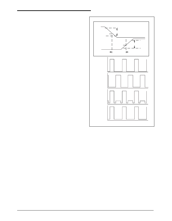
Gate Drivers
The SP6132 contains a pair of powerful 2
SOURCE and 1.5
SINK drivers. These state
of the art drivers are designed to drive external
NFETs capable of handling up to 30A. Rise,
fall, and non-overlap times have all been minized
to achieve maximum efficiency. All drive pins
GH, GL & SWN are monitored continuously to
ensure that only one external NFET is ever on at
any given time.
90%
10%
RISE TIME
2V
NON-OVERLAP
FALL TIME
2V
90%
10%
GH(GL)
GL(GH)
GATE DRIVER TEST CONDITIONS
V(BST)
GH
Voltage
V(VCC)
V(SWN)
GL
Voltage
V(VIN)
0V
-0V
-V(Diode) V
V(VIN)+V(VCC)
BST
Voltage
V(VCC)
TIME
SWN
Voltage
相關(guān)PDF資料 |
PDF描述 |
|---|---|
| SP6133 | Evaluation Board Manual |
| SP6133_06 | Evaluation Board Manual |
| SP6133EB | Evaluation Board Manual |
| SP6133ER1 | Evaluation Board Manual |
| SP61346 | Dual Supply Synchronous Buck Controller |
相關(guān)代理商/技術(shù)參數(shù) |
參數(shù)描述 |
|---|---|
| SP6133 | 制造商:SIPEX 制造商全稱:Sipex Corporation 功能描述:Evaluation Board Manual |
| SP6133_06 | 制造商:SIPEX 制造商全稱:Sipex Corporation 功能描述:Evaluation Board Manual |
| SP6133EB | 功能描述:DC/DC 開關(guān)控制器 Synchronous Buck Controller RoHS:否 制造商:Texas Instruments 輸入電壓:6 V to 100 V 開關(guān)頻率: 輸出電壓:1.215 V to 80 V 輸出電流:3.5 A 輸出端數(shù)量:1 最大工作溫度:+ 125 C 安裝風格: 封裝 / 箱體:CPAK |
| SP6133ER1 | 制造商:SIPEX 制造商全稱:Sipex Corporation 功能描述:Evaluation Board Manual |
| SP6133ER1/TR | 制造商:SIPEX 制造商全稱:Sipex Corporation 功能描述:Synchronous Buck Controller |
發(fā)布緊急采購,3分鐘左右您將得到回復。