- 您現(xiàn)在的位置:買賣IC網(wǎng) > PDF目錄299919 > SPT7835SIT (SIGNAL PROCESSING TECHNOLOGIES) 1-CH 10-BIT SUCCESSIVE APPROXIMATION ADC, PARALLEL ACCESS, PQFP32 PDF資料下載
參數(shù)資料
| 型號: | SPT7835SIT |
| 廠商: | SIGNAL PROCESSING TECHNOLOGIES |
| 元件分類: | ADC |
| 英文描述: | 1-CH 10-BIT SUCCESSIVE APPROXIMATION ADC, PARALLEL ACCESS, PQFP32 |
| 封裝: | TQFP-32 |
| 文件頁數(shù): | 12/12頁 |
| 文件大小: | 98K |
| 代理商: | SPT7835SIT |
SPT
9
5/15/01
SPT7835
Typically, the top side voltage drop for VRHF to VRHS will
equal:
VRHF – VRHS = 2.25 % of (VRHF – VRLF) (typical),
and the bottom side voltage drop for VRLS to VRLF will
equal:
VRLS – VRLF = 1.9 % of (VRHF – VRLF) (typical).
Figure 4 shows an example of expected voltage drops for
a specific case. VREF of 4.0 V is applied to VRHF, and VRLF
is tied to AGND. A 90 mV drop is seen at VRHS (= 3.91 V),
and a 75 mV increase is seen at VRLS (= 0.075 V).
ANALOG INPUT
VIN is the analog input. The input voltage range is from
VRLS to VRHS (typically 4.0 V) and will scale proportionally
with respect to the voltage reference. (See voltage refer-
ence section.)
The drive requirements for the analog inputs are very
minimal when compared to most other converters due to
the SPT7835’s extremely low input capacitance of only
5 pF and very high input resistance of 50 k
.
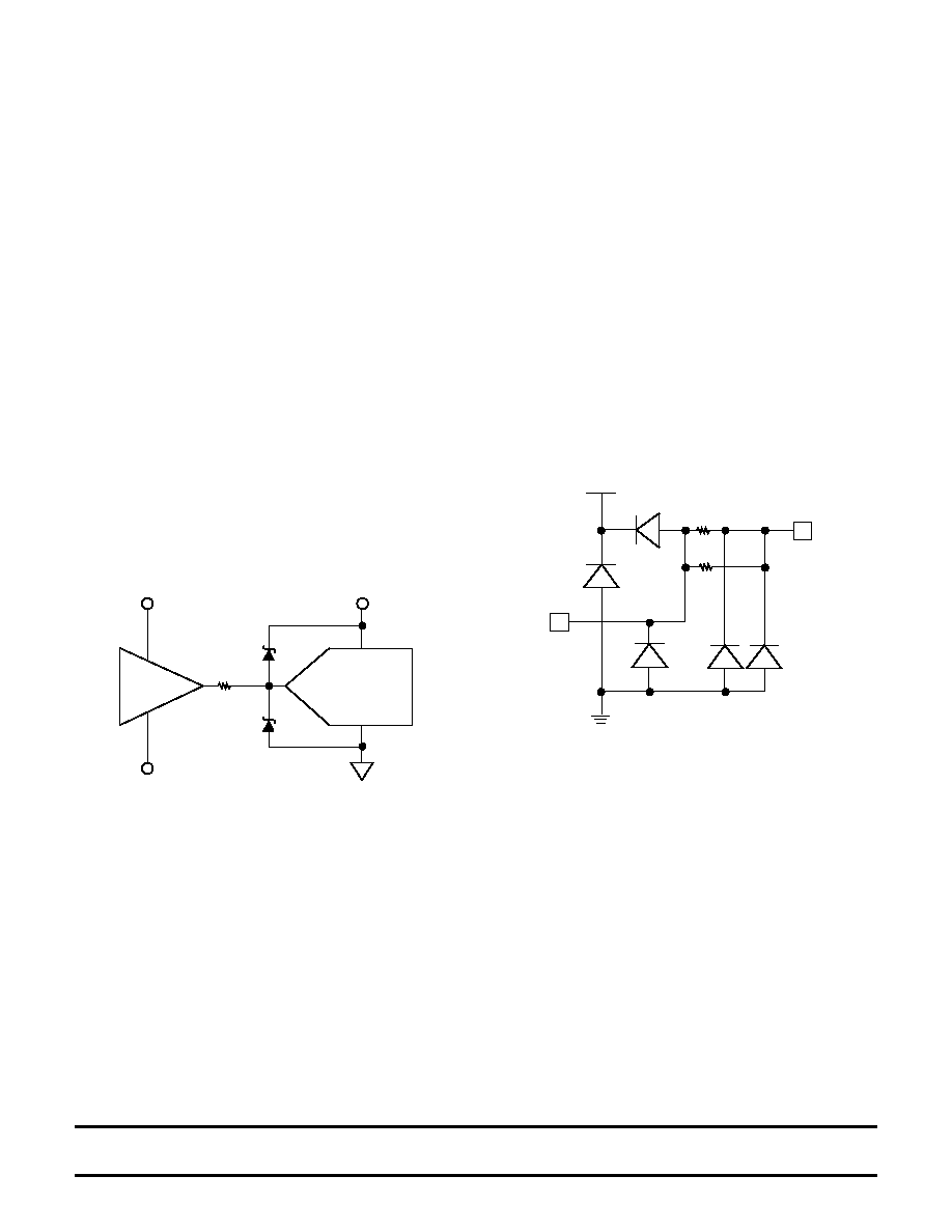
The analog input should be protected through a series
resistor and diode clamping circuit as shown in figure 5.
Upon powerup, the SPT7835 begins its calibration algo-
rithm. In order to achieve the calibration accuracy re-
quired, the offset and gain adjustment step size is a frac-
tion of a 10-bit LSB. Since the calibration algorithm is an
oversampling process, a minimum of 10,000 clock cycles
are required. This results in a minimum calibration time
upon powerup of 1 msec for a 5 MHz sample rate. Once
calibrated, the SPT7835 remains calibrated over time and
temperature.
Since the calibration cycles are initiated on the rising edge
of the clock, the clock must be continuously applied for the
SPT7835 to remain in calibration.
INPUT PROTECTION
All I/O pads are protected with an on-chip protection
circuit shown in figure 6. This circuit provides ESD robust-
ness to 3.5 kV and prevents latch-up under severe dis-
charge conditions without degrading analog transition
times.
Figure 5 – Recommended Input Protection Circuit
47 W
D1
D2
ADC
Buffer
AVDD
+V
V
D1 = D2 = Hewlett-Packard HP5712 or equivalent
Figure 6 – On-Chip Protection Circuit
VDD
Analog
Pad
120 W
CALIBRATION
The SPT7835 uses an auto-calibration scheme to ensure
10-bit accuracy over time and temperature. Gain and off-
set errors are continually adjusted to 10-bit accuracy
during device operation. This process is completely trans-
parent to the user.
POWER SUPPLY SEQUENCING CONSIDERATIONS
All logic inputs should be held low until power to the device
has settled to the specific tolerances. Avoid power decou-
pling networks with large time constants that could delay
VDD power to the device.
CLOCK INPUT
The SPT7835 is driven from a single-ended TTL-input
clock. Because the pipelined architecture operates on the
rising edge of the clock input, the device can operate over
a wide range of input clock duty cycles without degrading
the dynamic performance. The device’s sample rate is
1/2 of the input clock frequency. (See figure 1A timing
diagram.)
相關(guān)PDF資料 |
PDF描述 |
|---|---|
| SPT7855SCN | 1-CH 10-BIT SUCCESSIVE APPROXIMATION ADC, PARALLEL ACCESS, PDIP28 |
| SPT7855SCU | 1-CH 10-BIT SUCCESSIVE APPROXIMATION ADC, PARALLEL ACCESS, UUC |
| SPT7860SCS | 1-CH 10-BIT SUCCESSIVE APPROXIMATION ADC, PARALLEL ACCESS, PDSO28 |
| SPT7866SCR | 1-CH 10-BIT PROPRIETARY METHOD ADC, PARALLEL ACCESS, PDSO28 |
| SPT7910SCU | 1-CH 12-BIT FLASH/SUCCESSIVE APPROXIMATION ADC, PARALLEL ACCESS, UUC32 |
相關(guān)代理商/技術(shù)參數(shù) |
參數(shù)描述 |
|---|---|
| SPT7840 | 制造商:CADEKA 制造商全稱:CADEKA 功能描述:10-BIT, 10 MSPS, 100 mW A/D CONVERTER |
| SPT7840SCT | 制造商:FAIRCHILD 制造商全稱:Fairchild Semiconductor 功能描述:10-BIT, 10 MSPS, 100 mW A/D CONVERTER |
| SPT7840SIS | 制造商:FAIRCHILD 制造商全稱:Fairchild Semiconductor 功能描述:10-BIT, 10 MSPS, 100 mW A/D CONVERTER |
| SPT7850 | 制造商:FAIRCHILD 制造商全稱:Fairchild Semiconductor 功能描述:10-BIT, 20 MSPS, 140 mW A/D CONVERTER |
| SPT7850SCN | 制造商:FAIRCHILD 制造商全稱:Fairchild Semiconductor 功能描述:10-BIT, 20 MSPS, 140 mW A/D CONVERTER |
發(fā)布緊急采購,3分鐘左右您將得到回復。