- 您現(xiàn)在的位置:買賣IC網(wǎng) > PDF目錄299919 > SPT7866SCR (FAIRCHILD SEMICONDUCTOR CORP) 1-CH 10-BIT PROPRIETARY METHOD ADC, PARALLEL ACCESS, PDSO28 PDF資料下載
參數(shù)資料
| 型號(hào): | SPT7866SCR |
| 廠商: | FAIRCHILD SEMICONDUCTOR CORP |
| 元件分類: | ADC |
| 英文描述: | 1-CH 10-BIT PROPRIETARY METHOD ADC, PARALLEL ACCESS, PDSO28 |
| 封裝: | SSOP-28 |
| 文件頁數(shù): | 6/8頁 |
| 文件大小: | 59K |
| 代理商: | SPT7866SCR |
6
11/20/01
SPT7866
DIFFERENTIAL CLOCK INPUT
The SPT7866 clock can be driven differentially or single-
ended. When driven differentially, CLK and CLK accommo-
date differential sinusodial signals centered around VDD/2.
The peak-to-peak value should be 0.8 V. In order to pre-
serve accuracy at high input frequency, it is important that
the clock have low jitter. The differential clock input is made
to allow a low-jitter clock design. To ensure low jitter, the
differential input should be a pure sine wave with low white
noise floor.
SINGLE-ENDED CLOCK INPUT
For single-ended operation, the CLK node is internally
biased to 1.5 V, and should externally be decoupled to
ground by a capacitor. A CMOS logic level clock (5 V or
3 V) is applied at the CLK node. (To get an inverted clock
input, CLK should be decoupled and the clock signal ap-
plied at the CLK node). The duty cycle of the clock should
be close to 50%. Consecutive pipeline stages in the ADC
are clocked in antiphase. With a 50% duty cycle, every
stage has the same time for settling. If the duty cycle devi-
ates from 50%, every second stage has a shorter time for
settling; thus it operates less accurately, causing degrada-
tion of SNR.
In order to preserve accuracy at high input frequency, it is
important that the clock have low jitter and steep edges.
Rise/fall times should be kept shorter than 2 ns whenever
possible. Overshoot should be minimized. Low jitter is es-
pecially important when converting high-frequency input
signals. Jitter causes the noise floor to rise proportionally
to input signal frequency. Jitter may be caused by crosstalk
on the PCB. It is therefore recommended that the clock
trace on the PCB be made as short as possible.
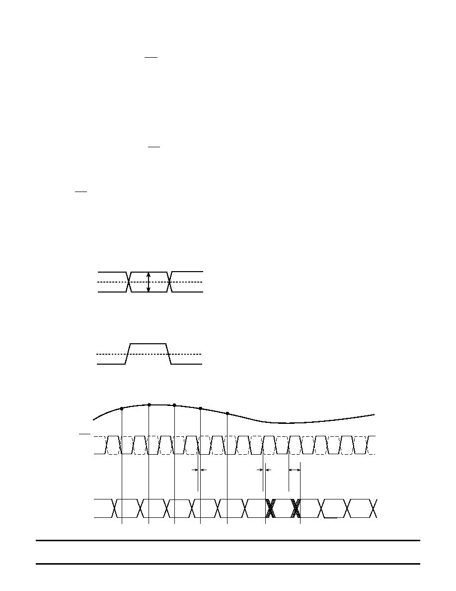
DIGITAL OUTPUTS
The digital output data appears in offset binary code at
CMOS logic levels. Full-scale negative input results in out-
put code 000...0. Full-scale positive input results in output
code 111...1. Output data is available 6 clock cycles after
the data is sampled. The analog input is sampled one
aperture delay (tAP) after the high-to-low clock transition.
Output data should be sampled as shown in the timing dia-
gram (figure 5). The OR pin is an out-of-range pin; if the
outputs go either over or under range, OR is set high.
PCB LAYOUT AND DECOUPLING
A well designed PCB is necessary to get good spectral
purity from any high-performance ADC. A multilayer PCB
with a solid ground plane is recommended for optimum
performance. If the system has a split analog and digital
ground plane, it is recommended that all ground pins on
the ADC be connected to the analog ground plane. It is our
experience that this gives the best performance. The
power supply pins should be bypassed using 100 nF
surface mounted capacitors as close to the package pins
as possible. Analog and digital supply pins should be
separately filtered.
Figure 3 – Driving Differential Inputs with a
Differential Configuration
Figure 4 – Driving Differential Inputs with a
Single-Ended Configuration
VIHD
VICM
VILD
VID
VIH
VICM
VIL
N1
N
N+1
N+2
N+3
Data
N1
Data
N
Data
N+1
Data
N+2
Data
Clock
tAP
tH
tD
AIN
Clock
Figure 5 – Timing Diagram
相關(guān)PDF資料 |
PDF描述 |
|---|---|
| SPT7910SCU | 1-CH 12-BIT FLASH/SUCCESSIVE APPROXIMATION ADC, PARALLEL ACCESS, UUC32 |
| SPT8100SCN | 18-BIT DELTA-SIGMA ADC, SERIAL ACCESS, PDIP32 |
| SPX1004S1-L-1-2/TR | 1-OUTPUT TWO TERM VOLTAGE REFERENCE, 1.235 V, PDSO8 |
| SPX1431N/TR | 1-OUTPUT TWO TERM VOLTAGE REFERENCE, 2.49 V, PBCY3 |
| SPX2810AM3-2.5/TR | 2.5 V FIXED POSITIVE LDO REGULATOR, 1.2 V DROPOUT, PDSO4 |
相關(guān)代理商/技術(shù)參數(shù) |
參數(shù)描述 |
|---|---|
| SPT7868 | 制造商:未知廠家 制造商全稱:未知廠家 功能描述:10-BIT,80 MSPS A/D CONVERTER |
| SPT7868SIR | 制造商:未知廠家 制造商全稱:未知廠家 功能描述:10-BIT,80 MSPS A/D CONVERTER |
| SPT7870 | 制造商:未知廠家 制造商全稱:未知廠家 功能描述:10-BIT, 100 MSPS ECL A/D CONVERTER |
| SPT7870SCU | 制造商:未知廠家 制造商全稱:未知廠家 功能描述:10-BIT, 100 MSPS ECL A/D CONVERTER |
| SPT7870SIQ | 制造商:未知廠家 制造商全稱:未知廠家 功能描述:10-BIT, 100 MSPS ECL A/D CONVERTER |
發(fā)布緊急采購(gòu),3分鐘左右您將得到回復(fù)。