- 您現(xiàn)在的位置:買賣IC網(wǎng) > PDF目錄10518 > SSM2166SZ-REEL7 (Analog Devices Inc)IC PREAMP AUDIO MONO MIC 14SOIC PDF資料下載
參數(shù)資料
| 型號: | SSM2166SZ-REEL7 |
| 廠商: | Analog Devices Inc |
| 文件頁數(shù): | 5/20頁 |
| 文件大?。?/td> | 0K |
| 描述: | IC PREAMP AUDIO MONO MIC 14SOIC |
| 產(chǎn)品變化通告: | Material Change 25/Mar/2009 |
| 標準包裝: | 1 |
| 類型: | AB 類 |
| 輸出類型: | 1-通道(單聲道) |
| 電源電壓: | 4.5 V ~ 5.5 V |
| 特點: | 麥克風 |
| 安裝類型: | 表面貼裝 |
| 供應商設備封裝: | 14-SOICN |
| 封裝/外殼: | 14-SOIC(0.154",3.90mm 寬) |
| 包裝: | 標準包裝 |
| 產(chǎn)品目錄頁面: | 775 (CN2011-ZH PDF) |
| 其它名稱: | SSM2166SZ-REEL7DKR |
Data Sheet
SSM2166
Rev. E | Page 13 of 20
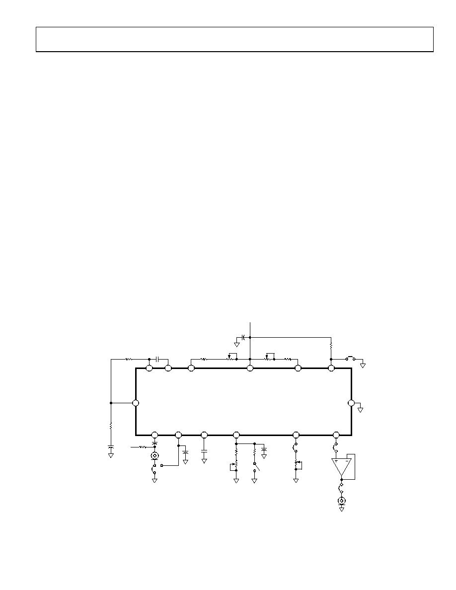
EVALUATION BOARD
A schematic diagram of the SSM2166 evaluation board is
illustrated in Figure 26. As a design aid, the layouts for the
topside silkscreen and the topside and backside metallization
layers are shown in Figure 27, Figure 28, and Figure 29. Although
not shown to scale, the finished dimension of the evaluation
board is 3.5 inches by 3.5 inches and comes complete with pin
sockets and a sample of the SSM2166.
Signal sources are connected to the SSM2166 through a 1/8-inch
phone jack where a 0.1 F capacitor couples the input signal
to the AUDIO +IN pin (Pin 7). As shown in Figure 26 and in
microphone applications, the phone jack shield can be optionally
connected to the ground plane of the board (Jumper J1 inserted
into the board socket for Pin 1 and Pin 2) or to the VCAR input
at Pin 4 (J1 inserted into the board socket for Pin 1 and Pin 3).
If the signal source is a waveform or function generator, the
phone jack shield should be connected to ground.
For ease in making adjustments for all configuration parameters,
single-turn potentiometers are used throughout. Optional Jumper
J2 connects the COMP RATIO SET pin to ground and sets the
SSM2166 for no compression (that is, compression ratio = 1:1).
Optional Jumper J3 connects the POWER DOWN (Pin 12) input
to ground for normal operation. J3 can be replaced by an open-
drain logic buffer for a digitally controlled shutdown function.
An output signal mute function can be implemented on the
SSM2166 by connecting the GAIN ADJUST pin (Pin 2) through a
330 resistance to ground. This is provided on the evaluation
board via R11 and S1. Capacitor C5, connected between Pin 2
and ground and provided on the evaluation board, can be used
to avoid audible clicks when using the mute function.
To configure the SSM2166 input buffer for gain, provisions for
R1, R2, and C2 have been included. To configure the input buffer
for unity-gain operation, R1 and R2 are removed and a direct
connection is made between the IN pin (Pin 6) and the BUF OUT
pin (Pin 5).
The output stage of the SSM2166 is capable of driving >1 V rms
(3 V p-p) into >5 k loads and is externally available through
an RCA phono jack provided on the board. If the output of the
SSM2166 is required to drive a lower load resistance or an audio
cable, the on-board OP113 can be used. To use the OP113 buffer,
insert Jumper J4 into the board socket for Pin 4 and Pin 5 and
insert Jumper J5 into the board socket for Pin 6 and Pin 7. If the
output buffer is not required, remove Jumper J5 and insert Jumper
J4 into board socket Pin 5 and Pin 7.
There are no blocking capacitors either on the input or at
the output of the buffer. As a result, the output dc level of the
buffer matches the output dc level of the SSM2166, which is
approximately 2.3 V. A dc blocking capacitor can be inserted at
Pin 6 and Pin 7. An evaluation board and setup procedure
is available from an Analog Devices, Inc., sales representative.
SSM2166
00357-
025
COMP
RATIO
ADJ
CW
R6
100k
5
4
6
7
OUTPUT
JACK
RCA
PHONO
OP113
R9
1k
R11
330
R10
20k
CW
GAIN
ADJ
MUTE
SWITCH
C5
0.01F
C4
22F
C7
10F
C1
0.1F
+
3
1
2
INPUT
JACK
1/8"
PHONE
MIC
PWR
C2
1F
R2
10k
C6
10F
C3
0.1F
R1
10k
+
R3
50k
CW
R7
1M
R8
500
R4
500
CCW
ROTATION
PT ADJ
+V
R12
100k
J3
NOISE GATE ADJ
4
8
7
2
13
10
1
6
POWER DOWN
NOISE GATE
SET
V+
ROTATION
SET
VCAIN
BUF OUT
AVG CAP
AUDIO +IN
GAIN ADJUST
COMP RATIO SET
3
5
14
12
9
11
–IN
VCAR
OUTPUT
GND
Figure 26. Evaluation Board Schematic
相關PDF資料 |
PDF描述 |
|---|---|
| LTC1419ACSW#PBF | IC A/D CONV 14BIT SAMPLNG 28SOIC |
| LTC1744CFW#PBF | IC ADC 14BIT 50MSPS 48-TSSOP |
| LTC2241CUP-10#PBF | IC ADC 10BIT 210MSPS 64-QFN |
| UP050B750K-KEC | CAP CER 75PF 50V 10% AXIAL |
| LTC2370CMS-16#PBF | IC ADC 16BIT SRL/SPI 2M 16-MSOP |
相關代理商/技術參數(shù) |
參數(shù)描述 |
|---|---|
| SSM2166SZ-REEL71 | 制造商:AD 制造商全稱:Analog Devices 功能描述:Microphone Preamplifier with Variable Compression and Noise Gating |
| SSM2166SZ-X | 制造商:Analog Devices 功能描述:MICROPHONE PREAMPLIFIER W/VAR COMPRESS, ROHS - Rail/Tube |
| SSM2167 | 制造商:AD 制造商全稱:Analog Devices 功能描述:Low Voltage Microphone Preamplifier with Variable Compression and Noise Gating |
| SSM2167_07 | 制造商:AD 制造商全稱:Analog Devices 功能描述:Low Voltage Microphone Preamplifier with Variable Compression and Noige Gating |
| SSM2167-1RM-R2 | 制造商:Rochester Electronics LLC 功能描述:MICROPHONE PREAMP W/ 18DB FIXED GAIN - Bulk 制造商:Analog Devices 功能描述:IC PREAMP AUDIO |
發(fā)布緊急采購,3分鐘左右您將得到回復。