- 您現(xiàn)在的位置:買賣IC網(wǎng) > PDF目錄11833 > ST16C654CQ64TR-F (Exar Corporation)IC UART FIFO 64B QUAD 64LQFP PDF資料下載
參數(shù)資料
| 型號(hào): | ST16C654CQ64TR-F |
| 廠商: | Exar Corporation |
| 文件頁(yè)數(shù): | 1/51頁(yè) |
| 文件大?。?/td> | 0K |
| 描述: | IC UART FIFO 64B QUAD 64LQFP |
| 標(biāo)準(zhǔn)包裝: | 1,000 |
| 特點(diǎn): | * |
| 通道數(shù): | 4,QUART |
| FIFO's: | 64 字節(jié) |
| 規(guī)程: | RS232 |
| 電源電壓: | 2.97 V ~ 5.5 V |
| 帶自動(dòng)流量控制功能: | 是 |
| 帶IrDA 編碼器/解碼器: | 是 |
| 帶故障啟動(dòng)位檢測(cè)功能: | 是 |
| 帶調(diào)制解調(diào)器控制功能: | 是 |
| 帶CMOS: | 是 |
| 安裝類型: | 表面貼裝 |
| 封裝/外殼: | 64-LQFP |
| 供應(yīng)商設(shè)備封裝: | 64-LQFP(10x10) |
| 包裝: | 帶卷 (TR) |
當(dāng)前第1頁(yè)第2頁(yè)第3頁(yè)第4頁(yè)第5頁(yè)第6頁(yè)第7頁(yè)第8頁(yè)第9頁(yè)第10頁(yè)第11頁(yè)第12頁(yè)第13頁(yè)第14頁(yè)第15頁(yè)第16頁(yè)第17頁(yè)第18頁(yè)第19頁(yè)第20頁(yè)第21頁(yè)第22頁(yè)第23頁(yè)第24頁(yè)第25頁(yè)第26頁(yè)第27頁(yè)第28頁(yè)第29頁(yè)第30頁(yè)第31頁(yè)第32頁(yè)第33頁(yè)第34頁(yè)第35頁(yè)第36頁(yè)第37頁(yè)第38頁(yè)第39頁(yè)第40頁(yè)第41頁(yè)第42頁(yè)第43頁(yè)第44頁(yè)第45頁(yè)第46頁(yè)第47頁(yè)第48頁(yè)第49頁(yè)第50頁(yè)第51頁(yè)
Exar Corporation 48720 Kato Road, Fremont CA, 94538 (510) 668-7000 FAX (510) 668-7017 www.exar.com
xr
ST16C654/654D
2.97V TO 5.5V QUAD UART WITH 64-BYTE FIFO
AUGUST 2005
REV. 5.0.2
GENERAL DESCRIPTION
The ST16C654/654D1 (654) is an enhanced quad
Universal Asynchronous Receiver and Transmitter
(UART) each with 64 bytes of transmit and receive
FIFOs, transmit and receive FIFO trigger levels,
automatic hardware and software flow control, and
data rates of up to 1.5 Mbps. Each UART has a set
of registers that provide the user with operating status
and control, receiver error indications, and modem
serial interface controls. Selectable interrupt polarity
provides flexibility to meet design requirements. An
internal
loopback
capability
allows
onboard
diagnostics. The 654 is available in 64 pin LQFP, 68
pin PLCC and 100 pin QFP packages. The 64 pin
package only offers the 16 mode interface, but the 68
and 100 pin packages offer an additional 68 mode
interface which allows easy integration with Motorola
processors.
The ST16C654CQ64 (64 pin) offers
three
state
interrupt
output
while
the
ST16C654DCQ64 provides continuous interrupt
output.
The 100 pin package provides additional
FIFO status outputs (TXRDY# and RXRDY# A-D),
separate infrared transmit data outputs (IRTX A-D)
and channel C external clock input (CHCCLK). The
ST16C654/654D is compatible with the industry
standard ST16C454 and ST16C654/554D.
NOTE: 1 Covered by U.S. Patent #5,649,122.
FEATURES
Pin-to-pin compatible with ST16C454, ST16C554
and TI’s TL16C554AFN and TL16C754BFN
Intel or Motorola Data Bus Interface select
Four independent UART channels
■ Register Set Compatible to 16C550
■ Data rates of up to 1.5 Mbps
■ 64 Byte Transmit FIFO
■ 64 Byte Receive FIFO with error tags
■ 4 Selectable TX and RX FIFO Trigger Levels
■ Automatic Hardware (RTS/CTS) Flow Control
■ Automatic Software (Xon/Xoff) Flow Control
■ Progammable Xon/Xoff characters
■ Wireless Infrared (IrDA 1.0) Encoder/Decoder
■ Full modem interface
2.97V to 5.5V supply operation
Sleep Mode (200 uA typical)
Crystal oscillator or external clock input
APPLICATIONS
Portable Appliances
Telecommunication Network Routers
Ethernet Network Routers
Cellular Data Devices
Factory Automation and Process Controls
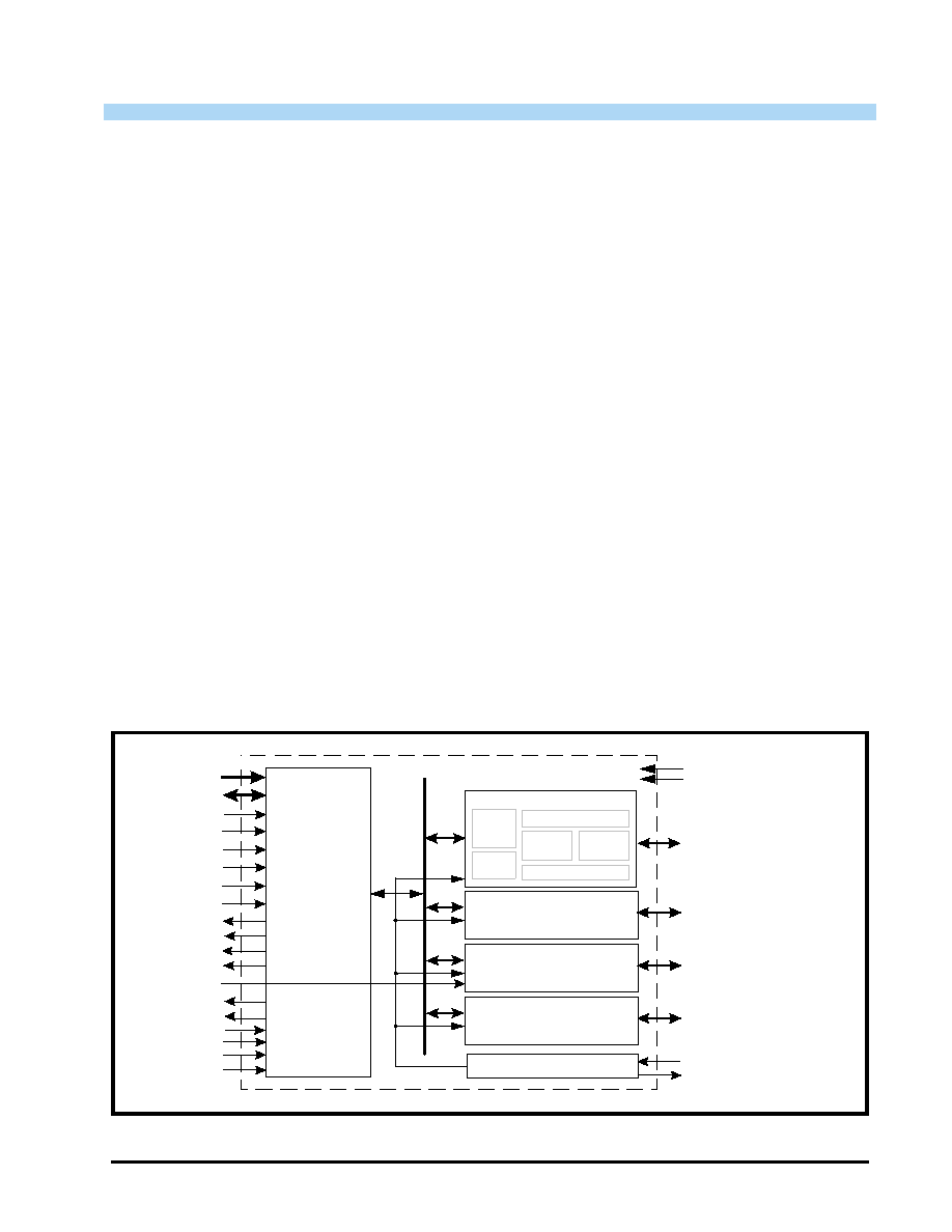
FIGURE 1. ST16C654 BLOCK DIAGRAM
XTAL1
XTAL2
Crystal Osc/Buffer
Data Bus
Interface
UART Channel A
64 Byte TX FIFO
64 Byte RX FIFO
BRG
IR
ENDEC
TX & RX
UART
Regs
2.97V to 5.5V VCC
GND
654 BLK
TXB, RXB, IRTXB, DTRB#,
DSRB#, RTSB#, CTSB#,
CDB#, RIB#
UART Channel B
(same as Channel A)
A2:A0
D7:D0
CSA#
16/68#
CSB#
INTA
INTB
IOW#
IOR#
Reset
INTSEL
CHCCLK
TXRDY# A-D
RXRDY# A-D
UART Channel C
(same as Channel A)
TXA, RXA, IRTXA, DTRA#,
DSRA#, RTSA#, CTSA#,
CDA#, RIA#
TXC, RXC, IRTXC, DTRC#,
DSRC#, RTSC#, CTSC#,
CDC#, RIC#
UART Channel D
(same as Channel A)
TXD, RXD, IRTXD, DTRD#,
DSRD#, RTSD#, CTSD#,
CDD#, RID#
CSC#
CSD#
INTC
INTD
CLKSEL
相關(guān)PDF資料 |
PDF描述 |
|---|---|
| XR16V564IV80-F | IC UART FIFO 32B QUAD 80LQFP |
| VE-25B-IY | CONVERTER MOD DC/DC 95V 50W |
| XR16M564IV80-F | IC UART FIFO 32B QUAD 80LQFP |
| VE-B5K-IX-F4 | CONVERTER MOD DC/DC 40V 75W |
| VE-B5K-IX-F3 | CONVERTER MOD DC/DC 40V 75W |
相關(guān)代理商/技術(shù)參數(shù) |
參數(shù)描述 |
|---|---|
| ST16C654D | 制造商:EXAR 制造商全稱:EXAR 功能描述:2.97V TO 5.5V QUAD UART WITH 64-BYTE FIFO |
| ST16C654DCQ64 | 制造商:Exar Corporation 功能描述: |
| ST16C654DCQ64-0A-EB | 功能描述:界面開發(fā)工具 Supports C654D 64 ld TQFP, ISA Interface RoHS:否 制造商:Bourns 產(chǎn)品:Evaluation Boards 類型:RS-485 工具用于評(píng)估:ADM3485E 接口類型:RS-485 工作電源電壓:3.3 V |
| ST16C654DCQ64-F | 功能描述:UART 接口集成電路 QUAD UARTW/64BYTE FIFO RoHS:否 制造商:Texas Instruments 通道數(shù)量:2 數(shù)據(jù)速率:3 Mbps 電源電壓-最大:3.6 V 電源電壓-最小:2.7 V 電源電流:20 mA 最大工作溫度:+ 85 C 最小工作溫度:- 40 C 封裝 / 箱體:LQFP-48 封裝:Reel |
| ST16C654DCQ64-F | 制造商:Exar Corporation 功能描述:IC QUAD UART 1.5MBPS 5.5V 64-LQFP |
發(fā)布緊急采購(gòu),3分鐘左右您將得到回復(fù)。