- 您現(xiàn)在的位置:買賣IC網(wǎng) > PDF目錄361357 > T81L0003B (TM Technology, Inc.) 8-bit MCU PDF資料下載
參數(shù)資料
| 型號: | T81L0003B |
| 廠商: | TM Technology, Inc. |
| 英文描述: | 8-bit MCU |
| 中文描述: | 8位微控制器 |
| 文件頁數(shù): | 6/16頁 |
| 文件大?。?/td> | 100K |
| 代理商: | T81L0003B |

TE
CH
tm
T81L0003B
8. Function Description
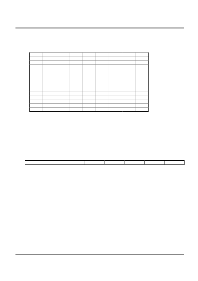
8.1. Special Function Register
F8H
F0H
B
E8H
E0H
ACC
D8H
D0H
PSW
C8H
T2CON T2MOD
C0H
B8H
IP
B0H
P3
A8H
IE
98H
SCON
90H
P1
88H
TCON TMOD
Accumulator : ACC
ACC is the Accumulator register. The mnemonics for Accumulator-Specific instructions, however, refer to the
Accumulator simply as A.
B Register : B
The B register is used during multiply and divide operations. For other instructions it can be treated as another scratch
pad register.
Program Status Word : PSW
The PSW register contains program status information as detailed in
CY
AC
F0
RS1
BIT SYMBOL FUNCTION
PSW.7 CY Carry flag.
PSW.6 AC Auxiliary Carry flag. (For BCD operations.)
PSW.5 F0 Flag 0. (Available to the user for general purposes.)
PSW.4 RS1 Register bank select control bit 1.
Set/cleared by software to determine working register bank. (See
Note.
)
PSW.3 RS0 Register bank select control bit 0.
Set/cleared by software to determine working register bank. (See
Note.
)
PSW.2 OV Overflow flag.
PSW.1 — User-definable flag.
PSW.0 P Parity flag.
Set/cleared by hardware each instruction cycle to indicate an odd/even number of “one” bits in the
Accumulator, i.e., even parity.
NOTE
: The contents of (RS1, RS0) enable the working register banks as follows:
(0,0)— Bank 0 (00H–07H)
(0,1)— Bank 1 (08H–0fH)
(1,0)— Bank 2 (10H–17H)
(1,1)— Bank 3 (18H–17H)
TM Technology Inc. reserves the right
P. 6
Publication Date: NOV. 2005
to change products or specifications without notice. Revision:A
TL2
TH0
TH2
TH1
SBUF
TL0
TL1
RS0
OV
--
P
相關(guān)PDF資料 |
PDF描述 |
|---|---|
| T81L0003B-AD | 8-bit MCU |
| T81L0003B-AK | 8-bit MCU |
| T81L0003B-BD | 8-bit MCU |
| T81L0003B-BK | 8-bit MCU |
| T81L0006A | 8-bit A/D Type MCU |
相關(guān)代理商/技術(shù)參數(shù) |
參數(shù)描述 |
|---|---|
| T81L0003B-AD | 制造商:TMT 制造商全稱:TMT 功能描述:8-bit MCU |
| T81L0003B-AK | 制造商:TMT 制造商全稱:TMT 功能描述:8-bit MCU |
| T81L0003B-BD | 制造商:TMT 制造商全稱:TMT 功能描述:8-bit MCU |
| T81L0003B-BK | 制造商:TMT 制造商全稱:TMT 功能描述:8-bit MCU |
| T81L0006A | 制造商:TMT 制造商全稱:TMT 功能描述:8-bit A/D Type MCU |
發(fā)布緊急采購,3分鐘左右您將得到回復(fù)。