- 您現(xiàn)在的位置:買賣IC網(wǎng) > PDF目錄371180 > T8538B T8538B Quad Programmable Codec PDF資料下載
參數(shù)資料
| 型號: | T8538B |
| 元件分類: | Codec |
| 英文描述: | T8538B Quad Programmable Codec |
| 中文描述: | T8538B四可編程編解碼器 |
| 文件頁數(shù): | 8/44頁 |
| 文件大小: | 847K |
| 代理商: | T8538B |
第1頁第2頁第3頁第4頁第5頁第6頁第7頁當(dāng)前第8頁第9頁第10頁第11頁第12頁第13頁第14頁第15頁第16頁第17頁第18頁第19頁第20頁第21頁第22頁第23頁第24頁第25頁第26頁第27頁第28頁第29頁第30頁第31頁第32頁第33頁第34頁第35頁第36頁第37頁第38頁第39頁第40頁第41頁第42頁第43頁第44頁
8
Agere Systems Inc.
Preliminary Data Sheet
August 2001
T8538B Quad Programmable Codec
Pin Information
(continued)
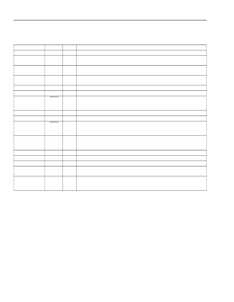
Table 4. Pin Assignments 64-Pin TQFP, Common Functions
Pin
Name
V
DD
DGND
Type
PWR
GND
Name/Description
1, 15, 27, 41, 55
2, 11, 32, 44, 56
Digital Power Supply (3.3 V).
Digital Ground.
Logic ground and return for logic power supply. A common
AGND, DGND plane is highly recommended.
PCM Frame Strobe Input.
This 8 kHz clock must be derived from the same
source as BCLK.
PCM Bit Clock Input.
This lead is used to develop internal clocks for cer-
tain clock rates.
PCM Transmit Data Output 0.
This is a 3-state output.
PCM Receive Data Input 0.
Backplane Line Driver Enable 0 (Active-Low).
Normally, these open-
drain outputs are floating in a high-impedance state. When a time slot is
active on DX0, this output pulls low to enable a backplane line driver.
PCM Transmit Data Output 1.
This a 3-state output.
PCM Receive Data Input 1.
Backplane Line Driver Enable 1 (Active-Low).
Normally, these open-
drain outputs are floating in a high-impedance state. When a time slot is
active on DX1, this output pulls low to enable a backplane line driver.
Power-On Reset.
A low causes a reset of the entire chip. This pin may be
connected to DGND with a 0.1
μ
F capacitor for a power-on reset function, or
it may be driven by external logic. This lead has an internal pull-up.
Serial Data Output.
This is a 3-state output.
Serial Data Input.
Serial Data Clock Input.
Chip Select Input.
This lead determines the interval that the serial interface
is active.
Serial Interface Select.
Leaving this lead open places the serial interface in
the normal mode; grounding it places the interface into the byte-by-byte
mode. This lead has an internal pull-up.
42
FS
I
43
BCLK
I
45
46
47
DX0
DR0
TSX0
O
I
O
48
49
50
DX1
DR1
TSX1
O
I
O
54
RST
I
57
58
59
60
DO
DI
DCLK
CS
O
I
I
I
61
INTS
I
相關(guān)PDF資料 |
PDF描述 |
|---|---|
| T923CFAA | T92-Type 10 Gbits/s 1300 nm Uncooled DFB Laser Transmitter |
| T923WFAA | T92-Type 10 Gbits/s 1300 nm Uncooled DFB Laser Transmitter |
| T923FFAA | T92-Type 10 Gbits/s 1300 nm Uncooled DFB Laser Transmitter |
| TBA120T | FM IF amplifier and demodulator |
| TBA120 | Sound I.F. amplifier/demodulator for TV |
相關(guān)代理商/技術(shù)參數(shù) |
參數(shù)描述 |
|---|---|
| T85471G | 制造商:BITECH 制造商全稱:Bi technologies 功能描述:Thick Film Super Low Profile SIP Resistor Networks |
| T85471J | 制造商:BITECH 制造商全稱:Bi technologies 功能描述:Thick Film Super Low Profile SIP Resistor Networks |
| T8550VBAAA | 制造商:Arcolectric 功能描述:2 Pole Miniature rocker switch(Curved) 制造商:Arcolectric 功能描述:Double Pole,Miniature rocker switch(Curved),Standard Body with Terminal Barrier |
| T8553VBNAK | 制造商:Arcolectric 功能描述:Double Pole,Miniature rocker switch(Curved lit),Standard Body with Terminal Barrier 制造商:Arcolectric 功能描述:2 Pole Mini rocker switch(Curved lit) |
| T85751B | 制造商:ITF 制造商全稱:ITF 功能描述:857.5 MHz SAW Filter |
發(fā)布緊急采購,3分鐘左右您將得到回復(fù)。