- 您現(xiàn)在的位置:買賣IC網(wǎng) > PDF目錄373617 > TDA2030AV (意法半導(dǎo)體) 18W Hi-Fi AMPLIFIER AND 35W DRIVER PDF資料下載
參數(shù)資料
| 型號(hào): | TDA2030AV |
| 廠商: | 意法半導(dǎo)體 |
| 元件分類: | 音頻放大器 |
| 英文描述: | 18W Hi-Fi AMPLIFIER AND 35W DRIVER |
| 中文描述: | 18W高保真放大器和35W的驅(qū)動(dòng) |
| 文件頁(yè)數(shù): | 13/15頁(yè) |
| 文件大?。?/td> | 238K |
| 代理商: | TDA2030AV |
第1頁(yè)第2頁(yè)第3頁(yè)第4頁(yè)第5頁(yè)第6頁(yè)第7頁(yè)第8頁(yè)第9頁(yè)第10頁(yè)第11頁(yè)第12頁(yè)當(dāng)前第13頁(yè)第14頁(yè)第15頁(yè)
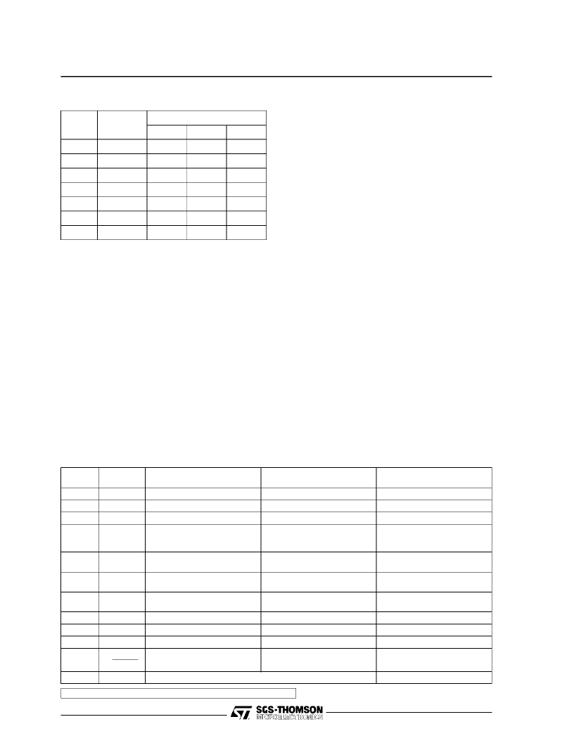
Table 2
Comp.
Recom.
Value
22k
680
22k
1
Purpose
Larger than
Recommended Value
Increase of gain
Decrease of gain (*)
Increase of input impedance
Danger of oscillation at high
frequencies with inductive
loads
Poor High Frequencies
Attenuation
Smaller than
Recommended Value
Decrease of gain
Increase of gain
Decrease of input impedance
R1
R2
R3
R4
Closed loop gain setting
Closed loop gain setting
Non inverting input biasing
Frequency Stability
R5
3 R2
Upper Frequency Cut-off
Danger of Oscillation
C1
1
μ
F
Input DC Decoupling
Increase of low frequencies
cut-off
Increase of low frequencies
cut-off
Danger of Oscillation
Danger of Oscillation
Larger Bandwidth
Larger Bandwidth
C2
22
μ
F
Inverting DC Decoupling
C3, C4
C5, C6
C7
C8
0.1
μ
F
100
μ
F
0.22
μ
F
Supply Voltage Bypass
Supply Voltage Bypass
Frequency Stability
Upper Frequency Cut-off
≈
1
2
π
BR1
1N4001
Smaller Bandwidth
D1, D2
To protect the device against output voltage spikes
Table 1
Mains
(220V)
Secondary
Voltage
DC OutputVoltage (V
o
)
I
o
= 0
I
o
= 0.1A
I
o
= 1A
+ 20%
28.8V
43.2V
42V
37.5V
+ 15%
27.6V
41.4V
40.3V
35.8V
+ 10%
26.4V
39.6V
38.5V
34.2V
–
24V
36.2V
35V
31V
– 10%
21.6V
32.4V
31.5V
27.8V
– 15%
20.4V
30.6V
29.8V
26V
– 20%
19.2V
28.8V
28V
24.3V
Aregulatedsupplyisnot usuallyusedforthepower
outputstagesbecauseof its dimensioningmust be
donetaking into accountthe power to supply inthe
signal peaks.They are only a smallpercentage of
the total music signal, with consequently large
overdimensioningof the circuit.
Evenif with a regulatedsupplyhigheroutputpower
canbeobtained(V
S
is constantin all working condi-
tions), the additional cost and power dissipationdo
notusually justify itsuse. Usingnon-regulatedsup-
plies, there are fewer designe restriction. In fact,
when signal peaks are present, the capacitor filter
actsas a flywheelsupplyingthe required energy.
In average conditions, the continuouspower sup-
plied is lower. The music power/continuouspower
ratio is greater in this case than for the case of
regulated supplied, with space saving and cost
reduction.
(*) The value of closed loop gain must be higher than 24dB.
APPLICATION SUGGESTION
The recommendedvalues of the componentsare
those shown on application circuit of Figure 14.
Differentvaluescan be used.The Table2 can help
the designer.
SHORT CIRCUIT PROTECTION
The TDA2030Ahas an original circuit which limits
the current of the output transistors. This function
can be considered as being peak power limiting
rather than simple current limiting. It reduces the
possibility that the devicegets damaged duringan
accidentalshort circuit from AC output to ground.
THERMAL SHUT-DOWN
The presenceof a thermal limiting circuit offersthe
following advantages:
1.
An overload on the output (even if it is
permanent), or an above limit ambient
temperaturecan be easily supported since the
T
j
cannot be higher than 150
o
C.
2.
The heatsink can have a smaller factor of
safety compared with that of a conventional
circuit.Thereisnopossibility ofdevicedamage
due to high junction temperature. If for any
reason, the junction temperatureincreases up
to 150
o
C, the thermal shut-down simply
reduces the power dissipationand the current
consumption.
TDA2030A
13/15
相關(guān)PDF資料 |
PDF描述 |
|---|---|
| TDA2030H | Single Audio Amplifier |
| TDA2030V | Single Audio Amplifier |
| TDA2030 | Single Audio Amplifier |
| TDA2030A | Insulation Putty 1 1/2 inch x 60 inch RoHS Compliant: Yes |
| TDA2030 | 14W Hi-Fi Audio Amplifier(14W Hi-Fi 音頻放大器) |
相關(guān)代理商/技術(shù)參數(shù) |
參數(shù)描述 |
|---|---|
| TDA2030AV | 制造商:STMicroelectronics 功能描述:IC AUDIO AMP 18W |
| TDA2030H | 功能描述:音頻放大器 14W Hi-Fi Audio Amp RoHS:否 制造商:STMicroelectronics 產(chǎn)品:General Purpose Audio Amplifiers 輸出類型:Digital 輸出功率: THD + 噪聲: 工作電源電壓:3.3 V 電源電流: 最大功率耗散: 最大工作溫度: 安裝風(fēng)格:SMD/SMT 封裝 / 箱體:TQFP-64 封裝:Reel |
| TDA2030H | 制造商:STMicroelectronics 功能描述:IC AUDIO AMP 14W |
| TDA2030L-TA5-T | 制造商:UTC-IC 制造商全稱:UTC-IC 功能描述:14W HI-FI AUDIO AMPLIFIER |
| TDA2030L-TB5-T | 制造商:UTC-IC 制造商全稱:UTC-IC 功能描述:14W HI-FI AUDIO AMPLIFIER |
發(fā)布緊急采購(gòu),3分鐘左右您將得到回復(fù)。