- 您現(xiàn)在的位置:買(mǎi)賣(mài)IC網(wǎng) > PDF目錄373626 > TDA8922B (NXP Semiconductors N.V.) 2 X 50 W class-D power amplifier PDF資料下載
參數(shù)資料
| 型號(hào): | TDA8922B |
| 廠(chǎng)商: | NXP Semiconductors N.V. |
| 英文描述: | 2 X 50 W class-D power amplifier |
| 中文描述: | 2 × 50瓦D類(lèi)功率放大器 |
| 文件頁(yè)數(shù): | 30/32頁(yè) |
| 文件大小: | 201K |
| 代理商: | TDA8922B |
第1頁(yè)第2頁(yè)第3頁(yè)第4頁(yè)第5頁(yè)第6頁(yè)第7頁(yè)第8頁(yè)第9頁(yè)第10頁(yè)第11頁(yè)第12頁(yè)第13頁(yè)第14頁(yè)第15頁(yè)第16頁(yè)第17頁(yè)第18頁(yè)第19頁(yè)第20頁(yè)第21頁(yè)第22頁(yè)第23頁(yè)第24頁(yè)第25頁(yè)第26頁(yè)第27頁(yè)第28頁(yè)第29頁(yè)當(dāng)前第30頁(yè)第31頁(yè)第32頁(yè)
9397 750 13357
Koninklijke Philips Electronics N.V. 2004. All rights reserved.
Preliminary data sheet
Rev. 01 — 1 October 2004
30 of 32
Philips Semiconductors
TDA8922B
2
×
50 W class-D power amplifier
16.4 Package related soldering information
[1]
For more detailed information on the BGA packages refer to the (LF)BGA Application Note(AN01026); order a copy from your Philips
Semiconductors sales office.
[2]
All surface mount (SMD) packages are moisture sensitive. Depending upon the moisture content, the maximum temperature (with
respect to time) and body size of the package, there is a risk that internal or external package cracks may occur due to vaporization of
the moisture in them (the so called popcorn effect). For details, refer to the Drypack information in the Data Handbook IC26; Integrated
Circuit Packages; Section: Packing Methods
[3]
For SDIP packages, the longitudinal axis must be parallel to the transport direction of the printed-circuit board.
[4]
Hot bar soldering or manual soldering is suitable for PMFP packages.
[5]
These transparent plastic packages are extremely sensitive to reflow soldering conditions and must on no account be processed
through more than one soldering cycle or subjected to infrared reflow soldering with peak temperature exceeding 217
°
C
±
10
°
C
measured in the atmosphere of the reflow oven. The package body peak temperature must be kept as low as possible.
[6]
These packages are not suitable for wave soldering. On versions with the heatsink on the bottom side, the solder cannot penetrate
between the printed-circuit board and the heatsink. On versions with the heatsink on the top side, the solder might be deposited on the
heatsink surface.
[7]
If wave soldering is considered, then the package must be placed at a 45
°
angle to the solder wave direction. The package footprint
must incorporate solder thieves downstream and at the side corners.
[8]
Wave soldering is suitable for LQFP, QFP and TQFP packages with a pitch (e) larger than 0.8 mm; it is definitely not suitable for
packages with a pitch (e) equal to or smaller than 0.65 mm.
[9]
Wave soldering is suitable for SSOP, TSSOP, VSO and VSSOP packages with a pitch (e) equal to or larger than 0.65 mm; it is definitely
not suitable for packages with a pitch (e) equal to or smaller than 0.5 mm.
[10] Image sensor packages in principle should not be soldered. They are mounted in sockets or delivered pre-mounted on flex foil.
However, the image sensor package can be mounted by the client on a flex foil by using a hot bar soldering process. The appropriate
soldering profile can be provided on request.
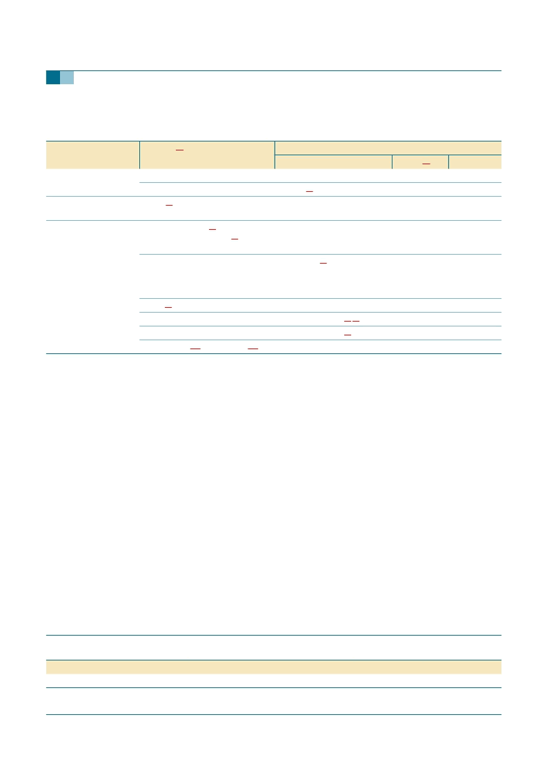
17. Revision history
Table 11:
Mounting
Suitability of IC packages for wave, reflow and dipping soldering methods
Package
[1]
Soldering method
Wave
suitable
suitable
[3]
not suitable
Reflow
[2]
not suitable
Dipping
suitable
Through-hole mount
CPGA, HCPGA
DBS, DIP, HDIP, RDBS, SDIP, SIL
PMFP
[4]
Through-hole-surface
mount
Surface mount
BGA, HTSSON..T
[5]
, LBGA,
LFBGA, SQFP, SSOP..T
[5]
,
TFBGA, VFBGA, XSON
DHVQFN, HBCC, HBGA, HLQFP,
HSO, HSOP, HSQFP, HSSON,
HTQFP, HTSSOP, HVQFN,
HVSON, SMS
PLCC
[7]
, SO, SOJ
LQFP, QFP, TQFP
SSOP, TSSOP, VSO, VSSOP
CWQCCN..L
[10]
, WQCCN..L
[10]
not suitable
suitable
not suitable
[6]
suitable
suitable
not recommended
[7] [8]
not recommended
[9]
not suitable
suitable
suitable
suitable
not suitable
Table 12:
Document ID
TDA8922B_1
Revision history
Release date
20041001
Data sheet status
Preliminary data sheet
Change notice
-
Order number
9397 750 13357
Supersedes
-
相關(guān)PDF資料 |
PDF描述 |
|---|---|
| TDA9102CT | H/V PROCESSOR FOR TTL V.D.U |
| TDA9102T | H/V PROCESSOR FOR TTL V.D.U |
| TDA9102F | H/V PROCESSOR FOR TTL V.D.U |
| TDA9102 | H/V PROCESSOR FOR TTL V.D.U |
| TDA9102C | H/V PROCESSOR FOR TTL V.D.U |
相關(guān)代理商/技術(shù)參數(shù) |
參數(shù)描述 |
|---|---|
| TDA8922BJ | 制造商:PHILIPS 制造商全稱(chēng):NXP Semiconductors 功能描述:2 X 50 W class-D power amplifier |
| TDA8922BJ/N2,112 | 功能描述:音頻放大器 2X50W CLASSD PWR AMP RoHS:否 制造商:STMicroelectronics 產(chǎn)品:General Purpose Audio Amplifiers 輸出類(lèi)型:Digital 輸出功率: THD + 噪聲: 工作電源電壓:3.3 V 電源電流: 最大功率耗散: 最大工作溫度: 安裝風(fēng)格:SMD/SMT 封裝 / 箱體:TQFP-64 封裝:Reel |
| TDA8922BTH | 制造商:PHILIPS 制造商全稱(chēng):NXP Semiconductors 功能描述:2 X 50 W class-D power amplifier |
| TDA8922BTH/N2,118 | 功能描述:音頻放大器 2X50W CLASSD PWR AMP RoHS:否 制造商:STMicroelectronics 產(chǎn)品:General Purpose Audio Amplifiers 輸出類(lèi)型:Digital 輸出功率: THD + 噪聲: 工作電源電壓:3.3 V 電源電流: 最大功率耗散: 最大工作溫度: 安裝風(fēng)格:SMD/SMT 封裝 / 箱體:TQFP-64 封裝:Reel |
| TDA8922BTH-T | 功能描述:音頻放大器 2X50W CLASSD PWR AMP RoHS:否 制造商:STMicroelectronics 產(chǎn)品:General Purpose Audio Amplifiers 輸出類(lèi)型:Digital 輸出功率: THD + 噪聲: 工作電源電壓:3.3 V 電源電流: 最大功率耗散: 最大工作溫度: 安裝風(fēng)格:SMD/SMT 封裝 / 箱體:TQFP-64 封裝:Reel |
發(fā)布緊急采購(gòu),3分鐘左右您將得到回復(fù)。