- 您現(xiàn)在的位置:買賣IC網(wǎng) > PDF目錄385925 > THS4302EVM (Texas Instruments, Inc.) THS4302 Evalutation Module(THS4302評估板) PDF資料下載
參數(shù)資料
| 型號: | THS4302EVM |
| 廠商: | Texas Instruments, Inc. |
| 英文描述: | THS4302 Evalutation Module(THS4302評估板) |
| 中文描述: | THS4302 Evalutation模塊(THS4302評估板) |
| 文件頁數(shù): | 18/25頁 |
| 文件大?。?/td> | 674K |
| 代理商: | THS4302EVM |
www.ti.com
DIE
Side View (a)
DIE
End View (b)
Bottom View (c)
0.144
0.056
0.144
0.010
vias
Pin 1
Top View
0.012
0.030
0.069
0.015
0.0095
0.049
0.032
0.0245
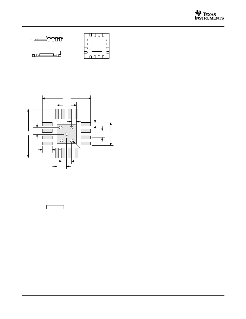
PowerPAD PCB LAYOUT
CONSIDERATIONS
1. Prepare the PCB with a top side etch pattern as
shown in Figure 50. There should be etch for the
leads as well as etch for the thermal pad.
2. Place five holes in the area of the thermal pad.
They holes should be 13 mils in diameter. Keep
them small so that solder wicking through the
holes is not a problem during reflow.
3. Additional vias may be placed anywhere along
the thermal plane outside of the thermal pad
area. They help dissipate the heat generated by
the IC. These additional vias may be larger than
the 13-mil diameter vias directly under the ther-
mal pad. They can be larger because they are
not in the thermal pad area to be soldered, so
that wicking is not a problem.
4. Connect all holes to the internal ground plane.
5. When connecting these holes to the ground
plane,
do not
use the typical web or spoke via
connection methodology. Web connections have
THERMAL ANALYSIS
The THS4302 device does not incorporate automatic
thermal shutoff protection, so the designer must take
care to ensure that the design does not violate the
absolute maximum junction temperature of the de-
vice. Failure may result if the absolute maximum
junction temperature of 150
°
C is exceeded.
THS4302
SLOS403F–OCTOBER 2002–REVISED FEBRUARY 2004
a high thermal resistance connection that is
useful
for
slowing
the
soldering operations. This resistance makes the
soldering of vias that have plane connections
easier. In this application, however, low thermal
resistance is desired for the most efficient heat
transfer. Therefore, the holes under the IC
PowerPAD package should make their connec-
tion to the internal ground plane, with a complete
connection around the entire circumference of the
plated-through hole.
6. The top-side solder mask should leave the ter-
minals of the package and the thermal pad area
with its five holes exposed. The bottom-side
solder mask should cover the five holes of the
thermal pad area. This prevents solder from
being pulled away from the thermal pad area
during the reflow process.
7. Apply solder paste to the exposed thermal pad
area and all of the IC terminals.
8. With these preparatory steps in place, the IC is
simply placed in position and run through the
solder
reflow
operation
surface-mount component. This results in a part
that is properly installed.
heat
transfer
during
Figure 49. Views of Thermally Enhanced Package
Although there are many ways to properly heatsink
the PowerPAD package, the following steps illustrate
the recommended approach.
as
any
standard
The next consideration is the package constraints.
The two sources of heat within an amplifier are
quiescent power and output power. The designer
should never forget about the quiescent heat gener-
ated within the device, especially multi-amplifier de-
vices. Because these devices have linear output
stages (Class AB), most of the heat dissipation is at
low output voltages with high output currents.
Figure 50. PowerPAD PCB Etch and Via Pattern
The other key factor when dealing with power dissi-
pation is how the devices are mounted on the PCB.
The PowerPAD devices are extremely useful for heat
dissipation.
But,
the
device
soldered to a copper plane to fully use the heat
dissipation properties of the PowerPAD. The SOIC
package, on the other hand, is highly dependent on
how it is mounted on the PCB. As more trace and
copper area is placed around the device,
decreases and the heat dissipation capability in-
creases. For a single package, the sum of the RMS
output currents and voltages should be used to
choose the proper package.
should
always
be
Θ
JA
18
相關(guān)PDF資料 |
PDF描述 |
|---|---|
| THS4500EVM | THS4500 Evalutation Module(THS4500評估板) |
| THS5661ADW | 12-BIT, 125 MSPS, CommsDACE DIGITAL-TO-ANALOG CONVERTER |
| THS5661APW | 12-BIT, 125 MSPS, CommsDACE DIGITAL-TO-ANALOG CONVERTER |
| THS5671ADW | 14-BIT, 125 MSPS, CommsDAC DIGITAL-TO-ANALOG CONVERTER |
| THS5671APW | 14-BIT, 125 MSPS, CommsDAC DIGITAL-TO-ANALOG CONVERTER |
相關(guān)代理商/技術(shù)參數(shù) |
參數(shù)描述 |
|---|---|
| THS4302RGTR | 功能描述:高速運算放大器 Wideband Fixed Gain Amplifier RoHS:否 制造商:Texas Instruments 通道數(shù)量:1 電壓增益 dB:116 dB 輸入補償電壓:0.5 mV 轉(zhuǎn)換速度:55 V/us 工作電源電壓:36 V 電源電流:7.5 mA 最大工作溫度:+ 85 C 安裝風(fēng)格:SMD/SMT 封裝 / 箱體:SOIC-8 封裝:Tube |
| THS4302RGTR | 制造商:Texas Instruments 功能描述:Operational Amplifier (Op-Amp) IC |
| THS4302RGTRG4 | 功能描述:高速運算放大器 Wideband Fixed Gain Amplifier RoHS:否 制造商:Texas Instruments 通道數(shù)量:1 電壓增益 dB:116 dB 輸入補償電壓:0.5 mV 轉(zhuǎn)換速度:55 V/us 工作電源電壓:36 V 電源電流:7.5 mA 最大工作溫度:+ 85 C 安裝風(fēng)格:SMD/SMT 封裝 / 箱體:SOIC-8 封裝:Tube |
| THS4302RGTT | 功能描述:高速運算放大器 Wideband Fixed Gain Amplifier RoHS:否 制造商:Texas Instruments 通道數(shù)量:1 電壓增益 dB:116 dB 輸入補償電壓:0.5 mV 轉(zhuǎn)換速度:55 V/us 工作電源電壓:36 V 電源電流:7.5 mA 最大工作溫度:+ 85 C 安裝風(fēng)格:SMD/SMT 封裝 / 箱體:SOIC-8 封裝:Tube |
| THS4302RGTTG4 | 功能描述:高速運算放大器 Wideband Fixed Gain Amplifier RoHS:否 制造商:Texas Instruments 通道數(shù)量:1 電壓增益 dB:116 dB 輸入補償電壓:0.5 mV 轉(zhuǎn)換速度:55 V/us 工作電源電壓:36 V 電源電流:7.5 mA 最大工作溫度:+ 85 C 安裝風(fēng)格:SMD/SMT 封裝 / 箱體:SOIC-8 封裝:Tube |
發(fā)布緊急采購,3分鐘左右您將得到回復(fù)。