- 您現(xiàn)在的位置:買賣IC網(wǎng) > PDF目錄385925 > THS7001PWP (Texas Instruments, Inc.) 70-MHz PROGRAMMABLE-GAIN AMPLIFIERS PDF資料下載
參數(shù)資料
| 型號(hào): | THS7001PWP |
| 廠商: | Texas Instruments, Inc. |
| 英文描述: | 70-MHz PROGRAMMABLE-GAIN AMPLIFIERS |
| 中文描述: | 70 - MHz的可編程增益放大器 |
| 文件頁數(shù): | 20/32頁 |
| 文件大小: | 597K |
| 代理商: | THS7001PWP |
第1頁第2頁第3頁第4頁第5頁第6頁第7頁第8頁第9頁第10頁第11頁第12頁第13頁第14頁第15頁第16頁第17頁第18頁第19頁當(dāng)前第20頁第21頁第22頁第23頁第24頁第25頁第26頁第27頁第28頁第29頁第30頁第31頁第32頁
THS7001, THS7002
70-MHz PROGRAMMABLE-GAIN AMPLIFIERS
SLOS214B – OCTOBER 1998 – REVISED AUGUST 1999
20
POST OFFICE BOX 655303
DALLAS, TEXAS 75265
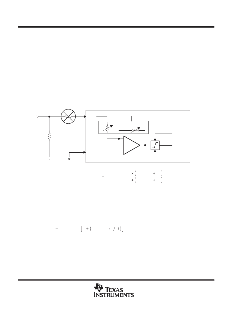
APPLICATION INFORMATION
PGA gain control (continued)
One aspect of the THS7001 and THS7002 PGA signal inputs is that there are internal variable resistors (R
F
and R
G
), which set the gain. The resistance of R
G
changes from about 270-
(Gain = +20 dB) to about 3-k
(Gain = –22 dB). Therefore, any source impedance at the input to the PGA amplifiers will cause a gain error
to be seen at the output. A buffer/amplifier is highly recommended to directly drive the input of the PGA section
to help minimize this effect.
Another thing which should be kept in mind is that when each amplifier’s V
REF
is connected to ground, the
internal R
G
resistor is connected to a virtual ground. Therefore, if a termination resistor is used on the source
side, the total terminating resistance is the parallel combination of the terminating resistance and the internal
R
G
resistor. This, in conjunction with the series impedance problem mentioned previously, can potentially cause
a voltage mismatch between the output of a 50-
source and the expected PGA output voltage. These points
can be easily seen in the simplified diagram of the THS7001 and THS7002 PGA section (see Figure 56).
+
–
PGA
VOUT
No Source Impedance
VIN
RG
RF
PGA
G0 G1 G2
PGA
–VIN
Negative
Clamp VL
Positive
Clamp VH
THS7001 and THS7002 IC
PGA
VREF
RTERMINATION
RSOURCE
RTOTAL TERMINATION
RTERMINATION
RTERMINATION
RSOURCE
RSOURCE
RG
RG
Figure 56. Simplified PGA Section of the THS7001 and THS7002
voltage reference terminal
If a voltage is applied to the PGA’s V
REF
terminal, then the output of the PGA section will amplify the applied
reference voltage by one plus the selected gain. Thus, the output gain strictly due to V
REF
will be from +0.6 dB
to +21 dB according to the following formula:
VOUT
VREF
20 X Log
10
1
PGA Gain V V
For most configurations, it is recommended that this pin be connected to the signal ground.
相關(guān)PDF資料 |
PDF描述 |
|---|---|
| THS7002EVM | 70-MHz PROGRAMMABLE-GAIN AMPLIFIERS |
| THS7002PWP | 70-MHz PROGRAMMABLE-GAIN AMPLIFIERS |
| THS8133ATQFP | TRIPLE 10-BIT, 80 MSPS VIDEO D/A CONVERTER WITH TRI-LEVEL SYNC GENERATION |
| THS8133TQFP | TRIPLE 10-BIT, 80 MSPS VIDEO D/A CONVERTER WITH TRI-LEVEL SYNC GENERATION |
| THS8134ATQFP | TRIPLE 8-BIT, 80 MSPS VIDEO D/A CONVERTER WITH TRI-LEVEL SYNC GENERATION |
相關(guān)代理商/技術(shù)參數(shù) |
參數(shù)描述 |
|---|---|
| THS7002 | 制造商:TI 制造商全稱:Texas Instruments 功能描述:70-MHz PROGRAMMABLE-GAIN AMPLIFIERS |
| THS7002CPWP | 功能描述:特殊用途放大器 70-MHz Programmable- Gain Dual RoHS:否 制造商:Texas Instruments 通道數(shù)量:Single 共模抑制比(最小值): 輸入補(bǔ)償電壓: 工作電源電壓:3 V to 5.5 V 電源電流:5 mA 最大功率耗散: 最大工作溫度:+ 70 C 最小工作溫度:- 40 C 安裝風(fēng)格:SMD/SMT 封裝 / 箱體:QFN-20 封裝:Reel |
| THS7002CPWPG4 | 功能描述:特殊用途放大器 70-MHz Hi-Spd Dual Prgrmbl-Gain Amp RoHS:否 制造商:Texas Instruments 通道數(shù)量:Single 共模抑制比(最小值): 輸入補(bǔ)償電壓: 工作電源電壓:3 V to 5.5 V 電源電流:5 mA 最大功率耗散: 最大工作溫度:+ 70 C 最小工作溫度:- 40 C 安裝風(fēng)格:SMD/SMT 封裝 / 箱體:QFN-20 封裝:Reel |
| THS7002CPWPR | 功能描述:特殊用途放大器 70-MHz Programmable- Gain Dual RoHS:否 制造商:Texas Instruments 通道數(shù)量:Single 共模抑制比(最小值): 輸入補(bǔ)償電壓: 工作電源電壓:3 V to 5.5 V 電源電流:5 mA 最大功率耗散: 最大工作溫度:+ 70 C 最小工作溫度:- 40 C 安裝風(fēng)格:SMD/SMT 封裝 / 箱體:QFN-20 封裝:Reel |
| THS7002CPWPRG4 | 功能描述:特殊用途放大器 70-MHz Programmable- Gain Dual RoHS:否 制造商:Texas Instruments 通道數(shù)量:Single 共模抑制比(最小值): 輸入補(bǔ)償電壓: 工作電源電壓:3 V to 5.5 V 電源電流:5 mA 最大功率耗散: 最大工作溫度:+ 70 C 最小工作溫度:- 40 C 安裝風(fēng)格:SMD/SMT 封裝 / 箱體:QFN-20 封裝:Reel |
發(fā)布緊急采購,3分鐘左右您將得到回復(fù)。