- 您現(xiàn)在的位置:買賣IC網(wǎng) > PDF目錄385925 > THS7001PWP (Texas Instruments, Inc.) 70-MHz PROGRAMMABLE-GAIN AMPLIFIERS PDF資料下載
參數(shù)資料
| 型號(hào): | THS7001PWP |
| 廠商: | Texas Instruments, Inc. |
| 英文描述: | 70-MHz PROGRAMMABLE-GAIN AMPLIFIERS |
| 中文描述: | 70 - MHz的可編程增益放大器 |
| 文件頁數(shù): | 21/32頁 |
| 文件大小: | 597K |
| 代理商: | THS7001PWP |
第1頁第2頁第3頁第4頁第5頁第6頁第7頁第8頁第9頁第10頁第11頁第12頁第13頁第14頁第15頁第16頁第17頁第18頁第19頁第20頁當(dāng)前第21頁第22頁第23頁第24頁第25頁第26頁第27頁第28頁第29頁第30頁第31頁第32頁
THS7001, THS7002
70-MHz PROGRAMMABLE-GAIN AMPLIFIERS
SLOS214B – OCTOBER 1998 – REVISED AUGUST 1999
21
POST OFFICE BOX 655303
DALLAS, TEXAS 75265
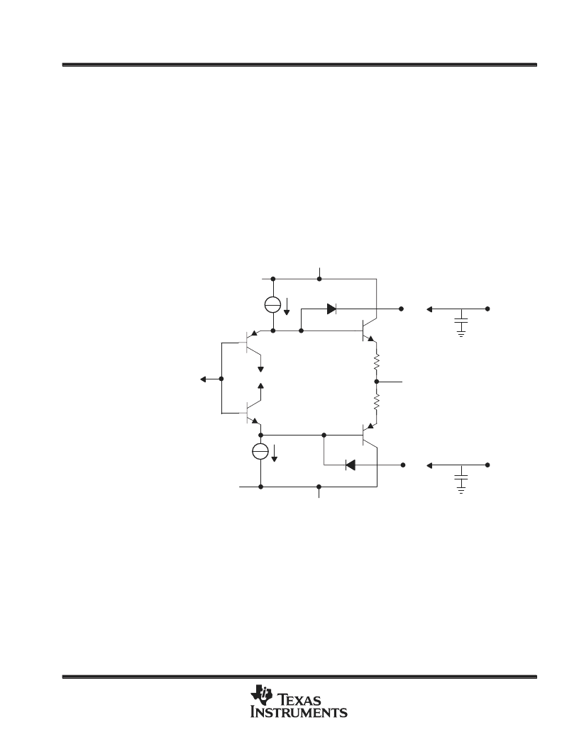
APPLICATION INFORMATION
output clamping
Typically, the output of the PGA will directly drive an analog-to-digital converter (ADC). Because of the limited
linear input range and saturation characteristics of most ADCs, the PGA’s outputs incorporate a voltage clamp.
Unlike a lot of clamping amplifiers which clamp only at the input, the THS7001 and THS7002 clamps at the
output stage. This insures that the output will always be protected regardless of the Gain setting and the input
voltage. The clamps activate almost instantaneously and recover from saturation in less than 7 ns. This can be
extremely important when the THS7001 and THS7002 is used to drive some ADCs which have a very long
overdrive recovery time. It is also recommended to add a pair of high frequency bypass capacitors to the clamp
inputs. These capacitors will help eliminate any ringing which may ocur when a large pulse is applied to the
amplifier. This pulse will force the clamp diodes to abruptly turn on, drawing current from the reference voltages.
Just like a power supply trace, you must minimize the inductance seen by the clamp pins. The bypass capacitors
will supply the sudden current demands when the clamps are suddenly turned on. A simplified clamping circuit
diagram is shown in Figure 57.
+VCC
–VCC
To Bias Circuits
VH
VL
OUT
Output
Transistor
Output
Transistor
Drive
V1
0.1
μ
F
V2
0.1
μ
F
Figure 57. Simplified THS7001 and THS7002 Clamp Circuit
Because the internal clamps utilize the same clamping reference voltages, the outputs of both PGAs on the
THS7002 are clamped to the same values. These clamps are typically connected to the power supply pins to
allow a full output range. But, they can be connected to any voltage reference desired. The clamping range is
limited to +V
CC
and GND for V
H
and –V
CC
and GND for V
L
. It is possible to go beyond GND for each respective
clamp, but it is not recommended. This is because this operation relies on the internal bias currents in the Class
AB output stage to maintain their linearity. There may also be a chance to reverse bias the PN junctions and
possibly cause internal damage to these junctions. But for reference, the graphs in Figure 58 show the output
voltage versus the clamping voltage with different loads.
相關(guān)PDF資料 |
PDF描述 |
|---|---|
| THS7002EVM | 70-MHz PROGRAMMABLE-GAIN AMPLIFIERS |
| THS7002PWP | 70-MHz PROGRAMMABLE-GAIN AMPLIFIERS |
| THS8133ATQFP | TRIPLE 10-BIT, 80 MSPS VIDEO D/A CONVERTER WITH TRI-LEVEL SYNC GENERATION |
| THS8133TQFP | TRIPLE 10-BIT, 80 MSPS VIDEO D/A CONVERTER WITH TRI-LEVEL SYNC GENERATION |
| THS8134ATQFP | TRIPLE 8-BIT, 80 MSPS VIDEO D/A CONVERTER WITH TRI-LEVEL SYNC GENERATION |
相關(guān)代理商/技術(shù)參數(shù) |
參數(shù)描述 |
|---|---|
| THS7002 | 制造商:TI 制造商全稱:Texas Instruments 功能描述:70-MHz PROGRAMMABLE-GAIN AMPLIFIERS |
| THS7002CPWP | 功能描述:特殊用途放大器 70-MHz Programmable- Gain Dual RoHS:否 制造商:Texas Instruments 通道數(shù)量:Single 共模抑制比(最小值): 輸入補(bǔ)償電壓: 工作電源電壓:3 V to 5.5 V 電源電流:5 mA 最大功率耗散: 最大工作溫度:+ 70 C 最小工作溫度:- 40 C 安裝風(fēng)格:SMD/SMT 封裝 / 箱體:QFN-20 封裝:Reel |
| THS7002CPWPG4 | 功能描述:特殊用途放大器 70-MHz Hi-Spd Dual Prgrmbl-Gain Amp RoHS:否 制造商:Texas Instruments 通道數(shù)量:Single 共模抑制比(最小值): 輸入補(bǔ)償電壓: 工作電源電壓:3 V to 5.5 V 電源電流:5 mA 最大功率耗散: 最大工作溫度:+ 70 C 最小工作溫度:- 40 C 安裝風(fēng)格:SMD/SMT 封裝 / 箱體:QFN-20 封裝:Reel |
| THS7002CPWPR | 功能描述:特殊用途放大器 70-MHz Programmable- Gain Dual RoHS:否 制造商:Texas Instruments 通道數(shù)量:Single 共模抑制比(最小值): 輸入補(bǔ)償電壓: 工作電源電壓:3 V to 5.5 V 電源電流:5 mA 最大功率耗散: 最大工作溫度:+ 70 C 最小工作溫度:- 40 C 安裝風(fēng)格:SMD/SMT 封裝 / 箱體:QFN-20 封裝:Reel |
| THS7002CPWPRG4 | 功能描述:特殊用途放大器 70-MHz Programmable- Gain Dual RoHS:否 制造商:Texas Instruments 通道數(shù)量:Single 共模抑制比(最小值): 輸入補(bǔ)償電壓: 工作電源電壓:3 V to 5.5 V 電源電流:5 mA 最大功率耗散: 最大工作溫度:+ 70 C 最小工作溫度:- 40 C 安裝風(fēng)格:SMD/SMT 封裝 / 箱體:QFN-20 封裝:Reel |
發(fā)布緊急采購,3分鐘左右您將得到回復(fù)。