- 您現(xiàn)在的位置:買賣IC網(wǎng) > PDF目錄383953 > TLC32040C (Texas Instruments, Inc.) ANALOG INTERFACE CIRCUITS PDF資料下載
參數(shù)資料
| 型號(hào): | TLC32040C |
| 廠商: | Texas Instruments, Inc. |
| 英文描述: | ANALOG INTERFACE CIRCUITS |
| 中文描述: | 模擬接口電路 |
| 文件頁(yè)數(shù): | 4/33頁(yè) |
| 文件大小: | 453K |
| 代理商: | TLC32040C |
第1頁(yè)第2頁(yè)第3頁(yè)當(dāng)前第4頁(yè)第5頁(yè)第6頁(yè)第7頁(yè)第8頁(yè)第9頁(yè)第10頁(yè)第11頁(yè)第12頁(yè)第13頁(yè)第14頁(yè)第15頁(yè)第16頁(yè)第17頁(yè)第18頁(yè)第19頁(yè)第20頁(yè)第21頁(yè)第22頁(yè)第23頁(yè)第24頁(yè)第25頁(yè)第26頁(yè)第27頁(yè)第28頁(yè)第29頁(yè)第30頁(yè)第31頁(yè)第32頁(yè)第33頁(yè)
TLC32040C, TLC32040I, TLC32041C, TLC32041I
ANALOG INTERFACE CIRCUITS
SLAS014E – SEPTEMBER 1987 – REVISED MAY 1995
4
POST OFFICE BOX 655303
DALLAS, TEXAS 75265
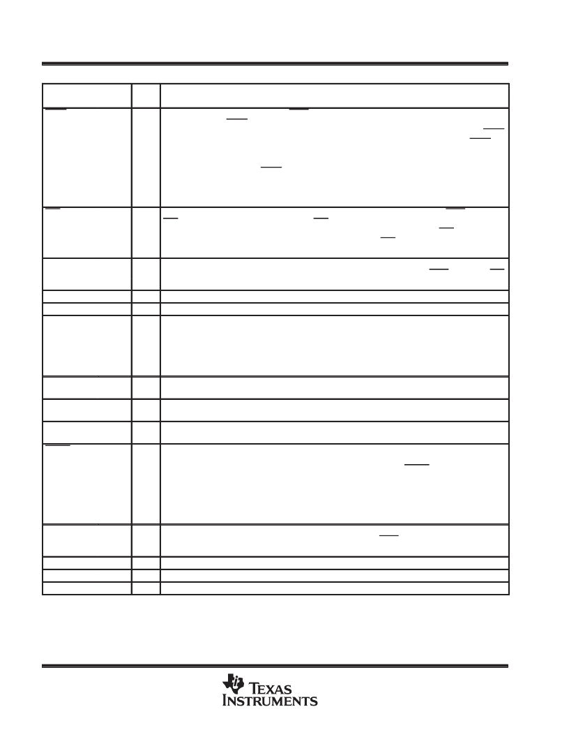
Terminal Functions (continued)
TERMINAL
I/O
DESCRIPTION
NAME
NO.
11
EODX
O
End of data transmit. See the WORD/BYTE description and the Serial Port Timing diagram. During the
word-mode timing, EODX is a low-going pulse that occurs immediately after the 16 bits of D/A converter
and control or register information have been transmitted from the TMS320 serial port to the AIC. EODX
can be used to interrupt a microprocessor upon the completion of serial communications. Also, EODX can
be used to strobe and enable external serial-to-parallel shift registers, latches, or an external FIFO RAM,
and to facilitate parallel data-bus communications between the AIC and the serial-to-parallel shift registers.
During the byte-mode timing, EODX goes low after the first byte has been transmitted from the TMS320
serial port to the AIC and is kept low until the second byte has been transmitted. The TMS32011 or
TMS320C17 can use this low-going signal to differentiate between the two bytes as to which is first and
which is second.
Frame sync receive. In the serial transmission modes, which are described in the WORD/BYTE description,
FSR is held low during bit transmission. When FSR goes low, the TMS320 serial port begins receiving bits
from the AIC via DR of the AIC. The most significant DR bit is present on DR before FSR goes low. (See
Serial Port Timing and Internal Timing Configuration diagrams.) FSR does not occur after secondary
communication.
Frame sync transmit. When FSX goes low, the TMS320 serial port begins transmitting bits to the AIC via
DX of the AIC. In all serial transmission modes, which are described in the WORD/BYTE description, FSX
is held low during bit transmission (see the Serial Port Timing and Internal Timing Configuration diagrams).
FSR
4
O
FSX
14
O
IN+
26
I
Noninverting input to analog input amplifier stage
IN–
25
I
Inverting input to analog input amplifier stage
MSTR CLK
6
I
Master clock. MSTR CLK is used to derive all the key logic signals of the AIC, such as the shift clock, the
switched-capacitor filter clocks, and the A/D and D/A timing signals. The Internal Timing Configuration
diagram shows how these key signals are derived. The frequencies of these key signals are synchronous
submultiples of the master clock frequency to eliminate unwanted aliasing when the sampled analog signals
are transferred between the switched-capacitor filters and the A/D and D/A converters (see the Internal
Timing Configuration).
OUT+
22
O
Noninverting output of analog output power amplifier. OUT+ can drive transformer hybrids or
high-impedance loads directly in either a differential or a single-ended configuration.
OUT–
21
O
Inverting output of analog output power amplifier. OUT– is functionally identical with and complementary
to OUT+.
REF
8
I/O
Internal voltage reference for the TLC32040. For the TLC32040 and TLC32041 an external voltage
reference can be applied to this terminal.
RESET
2
I
Reset. A reset function is provided to initialize the TA, TA’, TB, RA, RA’, RB, and control registers. This reset
function initiates serial communications between the AIC and DSP. The reset function initializes all AIC
registers including the control register. After a negative-going pulse on RESET, the AIC registers are
initialized to provide an 8-kHz data conversion rate for a 5.184-MHz master clock input signal. The
conversion rate adjust registers, TA’ and RA’, are reset to 1. The control register bits are reset as follows
(see AIC DX data word format section):
d7 = 1, d6 = 1, d5 = 1, d4 = 0, d3 = 0, d2 = 1
This initialization allows normal serial-port communication to occur between AIC and DSP.
SHIFT CLK
10
O
Shift clock. SHIFT CLK is obtained by dividing the master clock signal frequency by four. SHIFT CLK is used
to clock the serial data transfers of the AIC, described in the WORD/BYTE description below (see the Serial
Port Timing and Internal Timing Configuration diagrams).
VDD
VCC+
VCC–
7
Digital supply voltage, 5 V
±
5%
Positive analog supply voltage, 5 V
±
5%
Negative analog supply voltage, –5 V
±
5%
20
19
相關(guān)PDF資料 |
PDF描述 |
|---|---|
| TLC32040I | ANALOG INTERFACE CIRCUITS |
| TLC32041C | ANALOG INTERFACE CIRCUITS |
| TLC32041CFN | ANALOG INTERFACE CIRCUITS |
| TLC32041I | ANALOG INTERFACE CIRCUITS |
| TLC32040M | ANALOG INTERFACE CIRCUIT |
相關(guān)代理商/技術(shù)參數(shù) |
參數(shù)描述 |
|---|---|
| TLC32040CFN | 制造商:TI 制造商全稱:Texas Instruments 功能描述:ANALOG INTERFACE CIRCUITS |
| TLC32040CN | 制造商:TI 制造商全稱:Texas Instruments 功能描述:ANALOG INTERFACE CIRCUITS |
| TLC32040I | 制造商:TI 制造商全稱:Texas Instruments 功能描述:ANALOG INTERFACE CIRCUITS |
| TLC32040IN | 制造商:TI 制造商全稱:Texas Instruments 功能描述:ANALOG INTERFACE CIRCUITS |
| TLC32040M | 制造商:TI 制造商全稱:Texas Instruments 功能描述:ANALOG INTERFACE CIRCUIT |
發(fā)布緊急采購(gòu),3分鐘左右您將得到回復(fù)。