- 您現(xiàn)在的位置:買賣IC網(wǎng) > PDF目錄383953 > TLC32041C (Texas Instruments, Inc.) ANALOG INTERFACE CIRCUITS PDF資料下載
參數(shù)資料
| 型號: | TLC32041C |
| 廠商: | Texas Instruments, Inc. |
| 英文描述: | ANALOG INTERFACE CIRCUITS |
| 中文描述: | 模擬接口電路 |
| 文件頁數(shù): | 22/33頁 |
| 文件大小: | 453K |
| 代理商: | TLC32041C |
第1頁第2頁第3頁第4頁第5頁第6頁第7頁第8頁第9頁第10頁第11頁第12頁第13頁第14頁第15頁第16頁第17頁第18頁第19頁第20頁第21頁當(dāng)前第22頁第23頁第24頁第25頁第26頁第27頁第28頁第29頁第30頁第31頁第32頁第33頁
TLC32040C, TLC32040I, TLC32041C, TLC32041I
ANALOG INTERFACE CIRCUITS
SLAS014E – SEPTEMBER 1987 – REVISED MAY 1995
22
POST OFFICE BOX 655303
DALLAS, TEXAS 75265
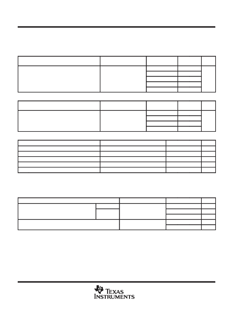
delay distortion, SCF clock frequency = 288 kHz
±
2%, input (IN+ – IN–) is
±
3-V sinewave
Refer to filter response graphs for delay distortion specifications.
TLC32040 and TLC32041 bandpass filter transfer function (see curves),
SCF clock frequency = 288 kHz,
±
2%, input (IN+ – IN–) is a
±
3-V sinewave
(see Note 9)
PARAMETER
TEST CONDITIONS
FREQUENCY
RANGE
MIN
MAX
UNIT
f = 100 Hz
–42
f = 170 Hz
300 Hz
≤
f
≤
3.4 kHz
f = 4 kHz
f
≥
4.6 kHz
–25
Filter gain, (see Note 10)
Input signal reference is 0 dB
–0.5
0.5
dB
–16
–58
low-pass filter transfer function, SCF clock frequency = 288 kHz
±
2% (see Note 9)
PARAMETER
TEST CONDITIONS
FREQUENCY
RANGE
f
≤
3.4 kHz
f = 3.6 kHz
MIN
MAX
UNIT
–0.5
0.5
Filter gain (see Note 10)
Filter gain, (see Note 10)
Output signal reference is 0 dB
–4
dB
f = 4 kHz
f
≥
4.4 kHz
–30
–58
serial port
PARAMETER
TEST CONDITIONS
MIN
TYP
MAX
UNIT
VOH
VOL
II
Ci
Co
High-level output voltage
IOH = –300
μ
A
IOL = 2 mA
2.4
V
Low-level output voltage
0.4
±
10
V
μ
A
pF
Input current
Input capacitance
15
Output capacitance
15
pF
operating characteristics over recommended operating free-air temperature range, V
CC+
= 5 V,
V
CC–
= –5 V, V
DD
= 5 V
noise (measurement includes low-pass and bandpass switched-capacitor filters)
PARAMETER
TEST CONDITIONS
MIN
TYP
MAX
UNIT
μ
V rms
μ
V rms
dBrncO
μ
V rms
dBrncO
Single ended
DX input = 00000000000000,
constant input code
constant in ut code
200
Transmit noise
Differential
300
500
20
Receive noise (see Note 11)
Inputs grounded,
gain = 1
300
20
475
All typical values are at TA = 25
°
C.
NOTES:
9. The above filter specifications are for a switched-capacitor filter clock range of 288 kHz
±
2%. For switched-capacitor filter clocks
at frequencies other than 288 kHz
±
2%, the filter response is shifted by the ratio of switched-capacitor filter clock frequency to
288 kHz.
10. The filter gain outside of the passband is measured with respect to the gain at 1 kHz. The filter gain within the passband is measured
with respect to the average gain within the passband. The passbands are 300 to 3400 Hz and 0 to 3400 Hz for the bandpass and
low-pass filters respectively.
11. The noise is reffered to the input with a buffer gain of one. If the buffer gain is two or four, the noise figure is correspondingly reduced.
The noise is computed by statistically evaluating the digital output of the A/D converter.
相關(guān)PDF資料 |
PDF描述 |
|---|---|
| TLC32041CFN | ANALOG INTERFACE CIRCUITS |
| TLC32041I | ANALOG INTERFACE CIRCUITS |
| TLC32040M | ANALOG INTERFACE CIRCUIT |
| TLC32040MFK | ANALOG INTERFACE CIRCUIT |
| TLC32040MJ | ANALOG INTERFACE CIRCUIT |
相關(guān)代理商/技術(shù)參數(shù) |
參數(shù)描述 |
|---|---|
| TLC32041CFN | 制造商:TI 制造商全稱:Texas Instruments 功能描述:ANALOG INTERFACE CIRCUITS |
| TLC32041CN | 制造商:TI 功能描述:32041 |
| TLC32041I | 制造商:TI 制造商全稱:Texas Instruments 功能描述:ANALOG INTERFACE CIRCUITS |
| TLC32041IN | 制造商:TI 制造商全稱:Texas Instruments 功能描述:ANALOG INTERFACE CIRCUITS |
| TLC32042EFN | 制造商:Rochester Electronics LLC 功能描述: |
發(fā)布緊急采購,3分鐘左右您將得到回復(fù)。