- 您現(xiàn)在的位置:買賣IC網(wǎng) > PDF目錄98252 > TLV320AIC10IPFB (TEXAS INSTRUMENTS INC) SPECIALTY CONSUMER CIRCUIT, PQFP48 PDF資料下載
參數(shù)資料
| 型號: | TLV320AIC10IPFB |
| 廠商: | TEXAS INSTRUMENTS INC |
| 元件分類: | 消費家電 |
| 英文描述: | SPECIALTY CONSUMER CIRCUIT, PQFP48 |
| 封裝: | GREEN, PLASTIC, TQFP-48 |
| 文件頁數(shù): | 7/57頁 |
| 文件大小: | 454K |
| 代理商: | TLV320AIC10IPFB |
第1頁第2頁第3頁第4頁第5頁第6頁當前第7頁第8頁第9頁第10頁第11頁第12頁第13頁第14頁第15頁第16頁第17頁第18頁第19頁第20頁第21頁第22頁第23頁第24頁第25頁第26頁第27頁第28頁第29頁第30頁第31頁第32頁第33頁第34頁第35頁第36頁第37頁第38頁第39頁第40頁第41頁第42頁第43頁第44頁第45頁第46頁第47頁第48頁第49頁第50頁第51頁第52頁第53頁第54頁第55頁第56頁第57頁

2–1
2 Functional Description
2.1
Device Functions
2.1.1
Operating Frequencies
The sampling frequency represented by the frequency of the primary communication is derived from the master clock
(MCLK) input with the following equation:
Fs = Sampling (conversion) frequency = MCLK/(256
× N), N = 1, 2..., 32
The inverse of the sampling frequency is the time between the falling edges of two successive primary frame-sync
signals. This time is the conversion period. For example, to set the conversion rate to 8 kHz, MCLK = 256
× N × 8000.
NOTE:The value of N is defined in control register 2 and its power-up value is 32.
2.1.2
ADC Signal Channel
Both IN (INP, INM) and AUX (AURXFP, AURXM) inputs can use the built-in antialiasing filter that can be bypassed
by writing a 1 to bit D5 of control register 1. The AUX input can also be connected to the general-purpose amplifier
A1 for general-purpose applications, such as electret-microphone interface and 2-to-4-wire hybrid interface, by
writing a 1 to bit D6 of control register 1. Bit D4 of control register 1 selects between IN or AUX for the ADC. The
selected input signal is amplified by the PGA and applied to the ADC input. The ADC converts the signal into
discrete-output digital words in 2s-complement data format, corresponding to the analog-signal value at sampling
time. These 16-bit (or 15-bit) digital words, representing sampled values of the analog input signal after PGA, are
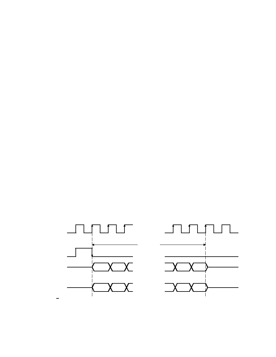
clocked out of the serial port (DOUT) at the positive edge of SCLK during the frame-sync (FS) interval at the rate of
one bit for each SCLK and one word for each primary communication. During secondary communication, the data
previously programmed into the registers can be read out. If a register read is not required, all 16 bits are cleared to
0 in the secondary communication. This read operation is accomplished by sending the appropriate register address
(D11-D9) with the read bit (D12) set to 1 during present secondary communication. The timing sequence is shown
in Figures 2–1 and 2–2.
The decimation FIR filter can be bypassed by writing a 1 to bit D2 of control register 1. The whole ADC channel can
be turned off for power savings by writing 01 to bits D2 and D1 of control register 3.
D0
16 SCLKs
SCLK
FS
DOUT
(16-bit)
DOUT
(15+1-bit)
D1
MSB
LSB
D15
M/S
D1
0
1
15
16
MSB
D15
D14
……
NOTES: A. M/S is used to indicate whether the 15-bit data comes from a master or a slave device (master: M/S=1, slave: M/S=0).
B. The MSB (D15) is stable (the host can latch the data in at this time) at the falling edging of SCLK number 0; the last bit (D0,M/S)
is stable at the falling edging of SCLK number 15.
Figure 2–1. Timing Sequence of ADC Channel (Primary Communication Only)
相關PDF資料 |
PDF描述 |
|---|---|
| TLV320AIC10CGQE | SPECIALTY CONSUMER CIRCUIT, PBGA80 |
| TLV320AIC10IGQE | SPECIALTY CONSUMER CIRCUIT, PBGA80 |
| TLV320AIC10CGQER | SPECIALTY CONSUMER CIRCUIT, PBGA80 |
| TLV320AIC10IGQER | SPECIALTY CONSUMER CIRCUIT, PBGA80 |
| TLV320AIC11C | SPECIALTY CONSUMER CIRCUIT, PQFP48 |
相關代理商/技術參數(shù) |
參數(shù)描述 |
|---|---|
| TLV320AIC10IPFBG4 | 功能描述:接口—CODEC 18-Bit Regstr Bus Trncvr W/3-St Otpt RoHS:否 制造商:Texas Instruments 類型: 分辨率: 轉換速率:48 kSPs 接口類型:I2C ADC 數(shù)量:2 DAC 數(shù)量:4 工作電源電壓:1.8 V, 2.1 V, 2.3 V to 5.5 V 最大工作溫度:+ 85 C 安裝風格:SMD/SMT 封裝 / 箱體:DSBGA-81 封裝:Reel |
| TLV320AIC10PFB | 制造商:TI 制造商全稱:Texas Instruments 功能描述:General-Purpose 3V to 5.5V 16-bit 22-KSPS DSP CODEC |
| TLV320AIC11 | 制造商:TI 制造商全稱:Texas Instruments 功能描述:General-Purpose Low-Voltage 1.1V to 3.6V/0 16-bit 22-KSPS DSP CODEC |
| TLV320AIC1103 | 制造商:TI 制造商全稱:Texas Instruments 功能描述:PCM CODEC |
| TLV320AIC1103EVM | 功能描述:音頻 IC 開發(fā)工具 TLV320AIC1103 Eval Mod RoHS:否 制造商:Texas Instruments 產(chǎn)品:Evaluation Kits 類型:Audio Amplifiers 工具用于評估:TAS5614L 工作電源電壓:12 V to 38 V |
發(fā)布緊急采購,3分鐘左右您將得到回復。