- 您現(xiàn)在的位置:買賣IC網(wǎng) > PDF目錄98252 > TLV320AIC22PTR (TEXAS INSTRUMENTS INC) SPECIALTY CONSUMER CIRCUIT, PQFP48 PDF資料下載
參數(shù)資料
| 型號: | TLV320AIC22PTR |
| 廠商: | TEXAS INSTRUMENTS INC |
| 元件分類: | 消費家電 |
| 英文描述: | SPECIALTY CONSUMER CIRCUIT, PQFP48 |
| 封裝: | ROHS COMPLIANT, PLASTIC, LQFP-48 |
| 文件頁數(shù): | 14/55頁 |
| 文件大小: | 782K |
| 代理商: | TLV320AIC22PTR |
第1頁第2頁第3頁第4頁第5頁第6頁第7頁第8頁第9頁第10頁第11頁第12頁第13頁當前第14頁第15頁第16頁第17頁第18頁第19頁第20頁第21頁第22頁第23頁第24頁第25頁第26頁第27頁第28頁第29頁第30頁第31頁第32頁第33頁第34頁第35頁第36頁第37頁第38頁第39頁第40頁第41頁第42頁第43頁第44頁第45頁第46頁第47頁第48頁第49頁第50頁第51頁第52頁第53頁第54頁第55頁

TLV320AIC22
DUAL VOIP CODEC
SLAS281B – JULY 2000 – REVISED JUNE 2002
21
POST OFFICE BOX 655303
DALLAS, TEXAS 75265
D DIN: the input serial data used to transfer DAC data and register control information from the attached DSP
serial interface (continued)
The TLV320AIC22 can be configured as a master or a slave. See the master/slave functionality section for a
detailed description. When configured as a master device, FSYNC and BCLK are generated by the master
codec and input to the DSP.
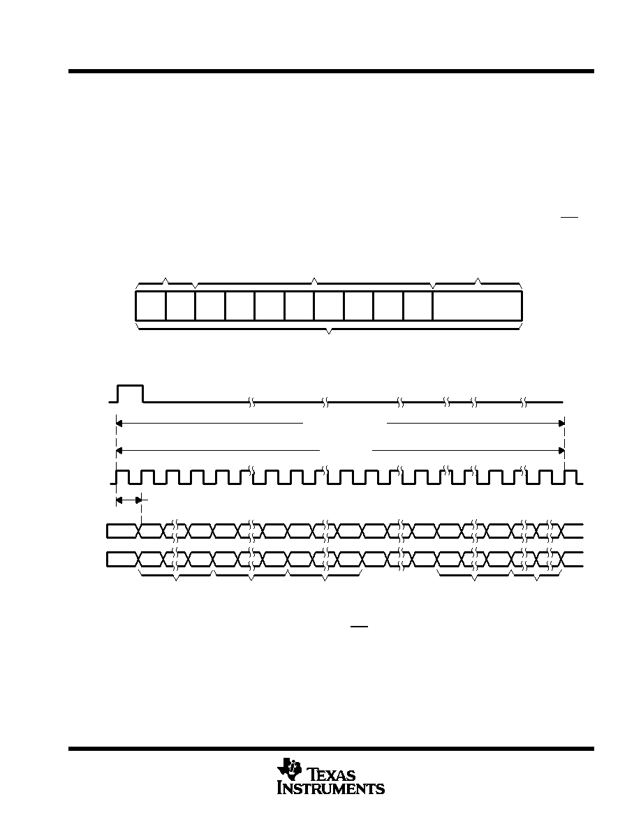
Data is received and transmitted in frames consisting of 256 BCLKs, which is 16, 16-bit time slots. Each frame
is subdivided into time slots, consisting of 16 BCLKs per time slot. In each frame, two time slots are reserved
for control-register information and eight time slots are reserved for codec data. The remaining six time slots
are unused. A pulse on the FSYNC pin indicates the beginning of a frame.
The control information is valid only when the serial interface has been selected by connecting the I2C/SPI pin
to logic 0. The frame format is shown in Figure 3, and the timing diagram for the frame is shown in Figure 4.
Time
Slot
0
Time
Slot
9
Time
Slot
8
Time
Slot
7
Time
Slot
6
Time
Slot
5
Time
Slot
4
Time
Slot
3
Time
Slot
2
Time
Slot
1
Time Slots 10–15
(unused)
256 BCLK Cycles
Control Register
Address and Data
Data
Vacant
Figure 3. Frame Format Used by the TLV320AIC22
FSYNC
DOUT
BCLK
15
0
16.384 MHz
15
0
Slot 0
Slot 9
Vacant
Slot 2
Slot 1
DIN
15
0
15
0
MSB
LSB MSB
LSB
MSB
LSB
One FSYNC Cycle
256 BCLKs
Figure 4. Timing Diagram for the TLV320AIC22 Frame Format
When the serial interface is selected for control (the I2C/SPI pin set to logic 0), the first two time slots after the
FSYNC pulse (time slots 0 and 1) are used for sending and receiving control data. The next eight slots are used
for actual conversion data sent and received by the codec.
Each time slot is 16 bits wide. Data bytes always are sent, with the first bit representing the MSB. Transmitted
data is sent on the rising edge of BCLK and data being received is latched on the falling edge of BCLK.
相關(guān)PDF資料 |
PDF描述 |
|---|---|
| TLV320AIC23BGQE | SPECIALTY CONSUMER CIRCUIT, PBGA80 |
| TLV320AIC23BIGQE | SPECIALTY CONSUMER CIRCUIT, PBGA80 |
| TLV320AIC23BIPW | SPECIALTY CONSUMER CIRCUIT, PDSO28 |
| TLV320AIC23BPW | SPECIALTY CONSUMER CIRCUIT, PDSO28 |
| TLV320AIC23BGQER | SPECIALTY CONSUMER CIRCUIT, PBGA80 |
相關(guān)代理商/技術(shù)參數(shù) |
參數(shù)描述 |
|---|---|
| TLV320AIC23 | 制造商:TI 制造商全稱:Texas Instruments 功能描述:STereo Audio CODEC, 8- to 96kHz, With Integrated Headphone Amplifier |
| TLV320AIC23_06 | 制造商:TI 制造商全稱:Texas Instruments 功能描述:Stereo Audio CODEC, 8-to 96-kHz, With Integrated Headphone Amplifier |
| TLV320AIC23B | 制造商:TI 制造商全稱:Texas Instruments 功能描述:Stereo Audio CODEC, 8-to 96-kHz, With Integrated Headphone Amplifier |
| TLV320AIC23B_06 | 制造商:TI 制造商全稱:Texas Instruments 功能描述:Stereo Audio CODEC, 8-to 96-kHz, With Integrated Headphone Amplifier |
| TLV320AIC23BGQE | 功能描述:接口—CODEC Lo-Pwr Highly Integrated Codec RoHS:否 制造商:Texas Instruments 類型: 分辨率: 轉(zhuǎn)換速率:48 kSPs 接口類型:I2C ADC 數(shù)量:2 DAC 數(shù)量:4 工作電源電壓:1.8 V, 2.1 V, 2.3 V to 5.5 V 最大工作溫度:+ 85 C 安裝風格:SMD/SMT 封裝 / 箱體:DSBGA-81 封裝:Reel |
發(fā)布緊急采購,3分鐘左右您將得到回復。