- 您現(xiàn)在的位置:買賣IC網(wǎng) > PDF目錄98252 > TLV320AIC22PTR (TEXAS INSTRUMENTS INC) SPECIALTY CONSUMER CIRCUIT, PQFP48 PDF資料下載
參數(shù)資料
| 型號(hào): | TLV320AIC22PTR |
| 廠商: | TEXAS INSTRUMENTS INC |
| 元件分類: | 消費(fèi)家電 |
| 英文描述: | SPECIALTY CONSUMER CIRCUIT, PQFP48 |
| 封裝: | ROHS COMPLIANT, PLASTIC, LQFP-48 |
| 文件頁(yè)數(shù): | 28/55頁(yè) |
| 文件大小: | 782K |
| 代理商: | TLV320AIC22PTR |
第1頁(yè)第2頁(yè)第3頁(yè)第4頁(yè)第5頁(yè)第6頁(yè)第7頁(yè)第8頁(yè)第9頁(yè)第10頁(yè)第11頁(yè)第12頁(yè)第13頁(yè)第14頁(yè)第15頁(yè)第16頁(yè)第17頁(yè)第18頁(yè)第19頁(yè)第20頁(yè)第21頁(yè)第22頁(yè)第23頁(yè)第24頁(yè)第25頁(yè)第26頁(yè)第27頁(yè)當(dāng)前第28頁(yè)第29頁(yè)第30頁(yè)第31頁(yè)第32頁(yè)第33頁(yè)第34頁(yè)第35頁(yè)第36頁(yè)第37頁(yè)第38頁(yè)第39頁(yè)第40頁(yè)第41頁(yè)第42頁(yè)第43頁(yè)第44頁(yè)第45頁(yè)第46頁(yè)第47頁(yè)第48頁(yè)第49頁(yè)第50頁(yè)第51頁(yè)第52頁(yè)第53頁(yè)第54頁(yè)第55頁(yè)
TLV320AIC22
DUAL VOIP CODEC
SLAS281B – JULY 2000 – REVISED JUNE 2002
34
POST OFFICE BOX 655303
DALLAS, TEXAS 75265
register programming using the I2C bus (continued)
SDA: I2C-bus serial address/data input/output. This is a bidirectional pin used to transfer register control
address and data into and out of the codec. It is an open-drain terminal and, therefore, requires a pullup
resistor to DVDD (typical 10 k
for 100 kHz).
AD0: In I2C mode, AD0 is a chip address bit.
AD1: In I2C mode, AD1 is a chip address bit.
Pins AD0 and AD1 form the partial chip address. The upper 5 bits (A6:A2) of the 7-bit address field must be
11100. To communicate with a TLV320AIC22, the LSBs of the chip address field (A1:A0), which is the first byte
sent to the TLV320AIC22, should match the settings of the AD1, AD0 pins. For normal data transfer, SDA is
allowed to change only during SCL low. Changes during SCL high are reserved for indicating the start and stop
conditions. Data transfer can be initiated only when the bus is not busy. During data transfer, the data line must
remain stable whenever the clock line is high. Changes in the data line while the clock line is high are interpreted
as a start or stop condition.
Table 14. I2C Bus Status
CONDITION
STATUS
DESCRIPTION
A
Bus not busy
Both data and clock lines remain high
B
Start data transfer
A high-to-low transition of the SDA line while the clock (SCL) is high determines a start condition. All
commands must proceed from a start condition.
C
Stop data transfer
A low-to-high transition of the SDA line while the clock (SCL) is high determines a stop condition. All
operations must end with a stop condition.
D
Data valid
The state of the data line represents valid data when, after a start condition, the data line is stable for the
duration of the high period of the clock signal.
I2C-bus conditions
The data on the line must be changed during the low period of the clock signal. There is one clock pulse per
bit data and each data transfer is initiated with a start condition and terminated with a stop condition. The host
device determines the number of data bytes transferred between the start and stop conditions. When
addressed, the TLV320AIC22 generates an acknowledge after the reception of each byte. The host device
(microprocessor or DSP) must generate an extra clock pulse which is associated with this acknowledge bit.
The TLV320AIC22 must pull the SDA line down during the acknowledge clock pulse, so that the SDA line is
stable low during the high period of the acknowledge-related clock pulse. Setup and hold times must be taken
into account. During reads, a host device must signal an end of data to the slave by not generating an
acknowledge bit on the last byte that has been clocked out of the slave. In this case, the slave (TLV320AIC22)
must leave the data line high to enable the host device to generate the stop condition.
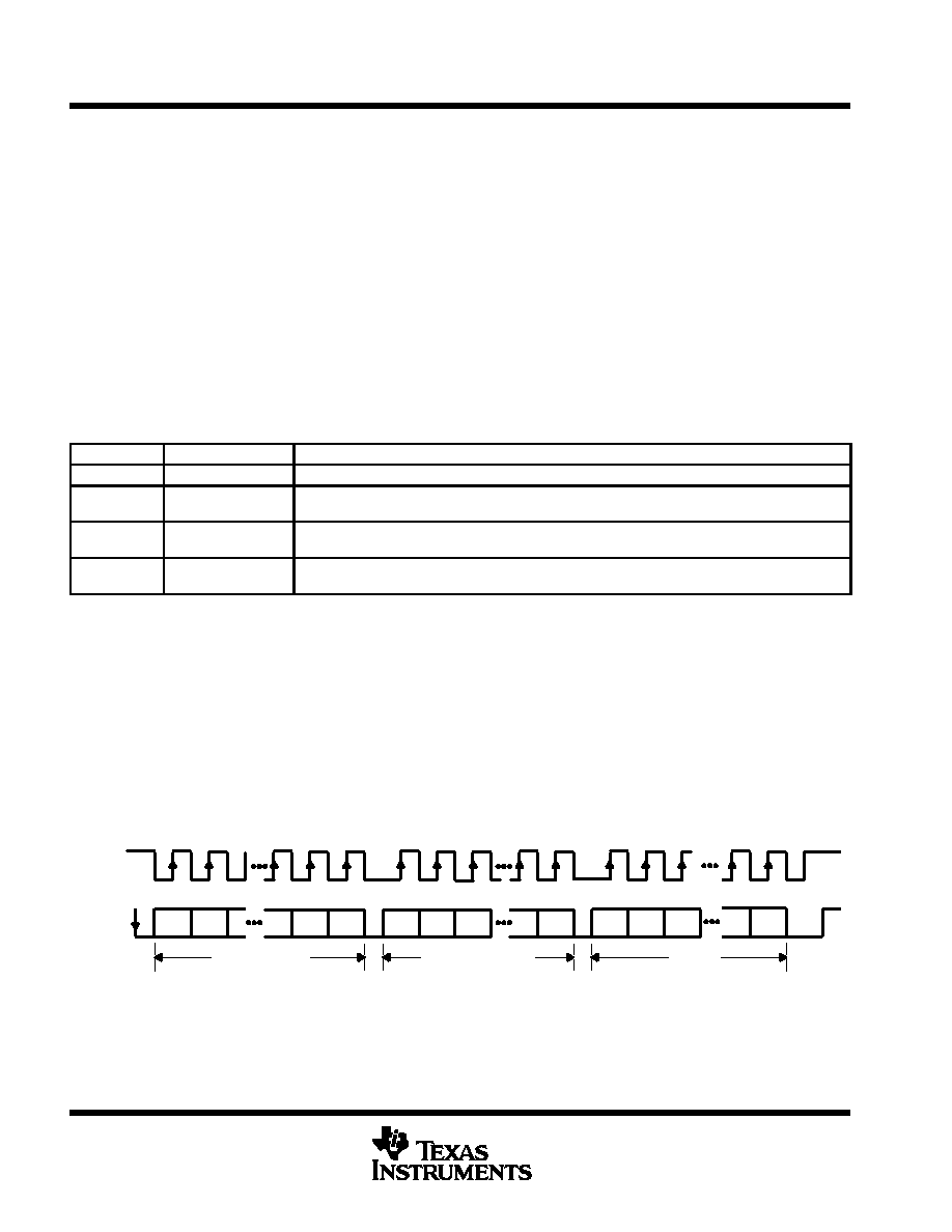
A0
R/W
00
Slave Address
00
SCL
SDA
Start
A6
A5
A4
ACK
R7
R6
R5
R0
ACK
D7
D6
D5
D0
ACK
Stop
Register Address
Data
Figure 16. I2C-Bus Write to TLV320AIC22
相關(guān)PDF資料 |
PDF描述 |
|---|---|
| TLV320AIC23BGQE | SPECIALTY CONSUMER CIRCUIT, PBGA80 |
| TLV320AIC23BIGQE | SPECIALTY CONSUMER CIRCUIT, PBGA80 |
| TLV320AIC23BIPW | SPECIALTY CONSUMER CIRCUIT, PDSO28 |
| TLV320AIC23BPW | SPECIALTY CONSUMER CIRCUIT, PDSO28 |
| TLV320AIC23BGQER | SPECIALTY CONSUMER CIRCUIT, PBGA80 |
相關(guān)代理商/技術(shù)參數(shù) |
參數(shù)描述 |
|---|---|
| TLV320AIC23 | 制造商:TI 制造商全稱:Texas Instruments 功能描述:STereo Audio CODEC, 8- to 96kHz, With Integrated Headphone Amplifier |
| TLV320AIC23_06 | 制造商:TI 制造商全稱:Texas Instruments 功能描述:Stereo Audio CODEC, 8-to 96-kHz, With Integrated Headphone Amplifier |
| TLV320AIC23B | 制造商:TI 制造商全稱:Texas Instruments 功能描述:Stereo Audio CODEC, 8-to 96-kHz, With Integrated Headphone Amplifier |
| TLV320AIC23B_06 | 制造商:TI 制造商全稱:Texas Instruments 功能描述:Stereo Audio CODEC, 8-to 96-kHz, With Integrated Headphone Amplifier |
| TLV320AIC23BGQE | 功能描述:接口—CODEC Lo-Pwr Highly Integrated Codec RoHS:否 制造商:Texas Instruments 類型: 分辨率: 轉(zhuǎn)換速率:48 kSPs 接口類型:I2C ADC 數(shù)量:2 DAC 數(shù)量:4 工作電源電壓:1.8 V, 2.1 V, 2.3 V to 5.5 V 最大工作溫度:+ 85 C 安裝風(fēng)格:SMD/SMT 封裝 / 箱體:DSBGA-81 封裝:Reel |
發(fā)布緊急采購(gòu),3分鐘左右您將得到回復(fù)。