- 您現(xiàn)在的位置:買賣IC網(wǎng) > PDF目錄368682 > TMS416100-60DJ x1 Fast Page Mode DRAM PDF資料下載
參數(shù)資料
| 型號: | TMS416100-60DJ |
| 英文描述: | x1 Fast Page Mode DRAM |
| 中文描述: | x1快速頁面模式的DRAM |
| 文件頁數(shù): | 3/25頁 |
| 文件大小: | 437K |
| 代理商: | TMS416100-60DJ |
TMS416100, TMS416100P
16777216-BIT
DYNAMIC RANDOM-ACCESS MEMORIES
SMKS611 – FEBRUARY 1994
3
POST OFFICE BOX 1443
HOUSTON, TEXAS 77251–1443
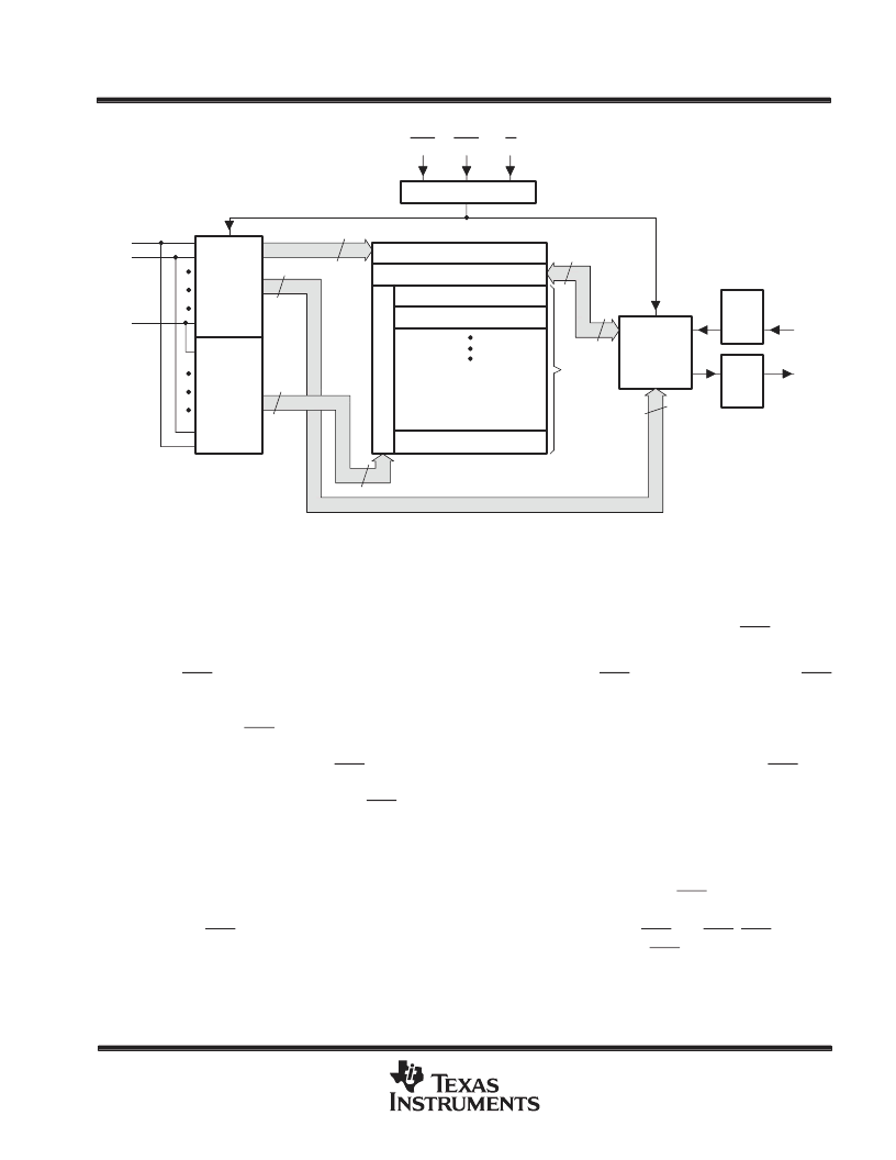
functional block diagram
A0
A1
A11
2
10
12
12
4
4
2
Timing and Control
Column-
Address
Buffers
Row-
Address
Buffers
I/O
Buffers
1 of 4
Selection
Data
In
Reg.
Data
Out
Reg.
Column Decode
Sense Amplifiers
64
256K Array
256K Array
256K Array
RAS
CAS
W
R
D
Q
operation
enhanced page mode
Enhanced page-mode operation allows faster memory access by keeping the same row address while selecting
random column addresses. The time for row-address setup and hold and address multiplex is thus eliminated.
The maximum number of columns that can be accessed is determined by t
RASP
, the maximum RAS-low time.
Unlike conventional page-mode DRAMs, the column-address buffers in this device are activated on the falling
edge of RAS. The buffers act as transparent or flow-through latches while CAS is high. The falling edge of CAS
latches the addresses and enables the output. This feature allows the TMS416100/P to operate at a higher data
bandwidth than conventional page-mode parts because retrieval begins as soon as the column address is valid
rather than when CAS transitions low. This performance improvement is referred to as enhanced page mode
Valid column address can be presented immediately after row-address hold time has been satisfied, usually well
in advance of the falling edge of CAS. In this case, data is obtained after t
CAC
max (access time from CAS low),
if t
AA
max (access time from column address) and t
RAC
have been satisfied. In the event that the column address
for the next cycle is valid at the time CAS goes high, access time for the next cycle is determined by the later
occurrence of t
CPA
or t
CAC
.
address (A0–A11)
Twenty-four address bits are required to decode 1 of 16777216 storage cell locations. Twelve row-address bits
are set up on inputs A0 through A11 and latched during a normal access and during RAS-only refresh as the
device requires 4096 refresh cycles. Twelve column-address bits are set up on inputs A0–A11 and latched onto
the chip by CAS. All addresses must be stable on or before the falling edges of RAS and CAS. RAS is similar
to a chip enable in that it activates the sense amplifiers as well as the row decoder. CAS is used as a chip select,
activating the output buffer as well as latching the address bits into the column-address buffer.
Powered by ICminer.com Electronic-Library Service CopyRight 2003
相關(guān)PDF資料 |
PDF描述 |
|---|---|
| TMS416100-60DZ | x1 Fast Page Mode DRAM |
| TMS416100-70DGA | x1 Fast Page Mode DRAM |
| TMS416100-70DJ | x1 Fast Page Mode DRAM |
| TMS416100-70DZ | x1 Fast Page Mode DRAM |
| TMS416100-80DGA | x1 Fast Page Mode DRAM |
相關(guān)代理商/技術(shù)參數(shù) |
參數(shù)描述 |
|---|---|
| TMS416100-60DZ | 制造商:未知廠家 制造商全稱:未知廠家 功能描述:x1 Fast Page Mode DRAM |
| TMS416100-70DGA | 制造商:未知廠家 制造商全稱:未知廠家 功能描述:x1 Fast Page Mode DRAM |
| TMS416100-70DJ | 制造商:未知廠家 制造商全稱:未知廠家 功能描述:x1 Fast Page Mode DRAM |
| TMS416100-70DZ | 制造商:未知廠家 制造商全稱:未知廠家 功能描述:x1 Fast Page Mode DRAM |
| TMS416100-80DGA | 制造商:未知廠家 制造商全稱:未知廠家 功能描述:x1 Fast Page Mode DRAM |
發(fā)布緊急采購,3分鐘左右您將得到回復(fù)。